 PCB
PCB FPC
FPC Rigid-Flex
 FR-4
FR-4 HDI PCB
 Rogers High-Frequency Board
 PTFE Teflon High-Frequency Board
 Aluminum
 Copper Core
 PCB Assembly
 LED light PCBA
 Memory PCBA
 Power Supply PCBA
 New Energey PCBA
 Communication PCBA
 Industrial Control PCBA
 Medical Equipment PCBA
 Testing Service
 PCBA Testing Service
 Certification Application
 RoHS Certification Application
 REACH Certification Application
 CE Certification Application
 FCC Certification Application
 CQC Certification Application
 UL Certification Application
 Transformers, Inductors
 High Frequency Transformers
 Low Frequency Transformers
 High Power Transformers
 Conversion Transformers
 Sealed Transformers
 Ring Transformers
 Inductors
 Wires,Cables Customized
 Network Cables
 Power Cords
 Antenna Cables
 Coaxial Cables
 Net Position Indicator
 Solar AIS net position indicator
 Capacitors
 Connectors
 Diodes
 Embedded Processors & Controllers
 Digital Signal Processors (DSP/DSC)
 Microcontrollers (MCU/MPU/SOC)
 Programmable Logic Device(CPLD/FPGA)
 Communication Modules/IoT
 Resistors
 Through Hole Resistors
 Resistor Networks, Arrays
 Potentiometers,Variable Resistors
 Aluminum Case,Porcelain Tube Resistance
 Current Sense Resistors,Shunt Resistors
 Switches
 Transistors
 Power Modules
 Isolated Power Modules
 AC-DC Power Modules
 DC-AC Module(Inverter)
 RF and Wireless
Mechanism of Copper Foil Roughness Impact on High-Frequency Signal Transmission
Mechanism of Copper Foil Roughness Impact on High-Frequency Signal Transmission
High-frequency signal transmission (>1 GHz) is highly sensitive to conductor suRFace properties. Copper foil roughness significantly affects signal integrity (SI) and insertion loss by altering current distribution under the skin effect, increasing surface scattering, and enhancing dielectric loss. The mechanisms are analyzed as follows:
I. Skin Effect and Current Path Distortion
-
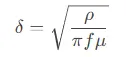
Skin Depth (δ) vs. Frequency:
-
: Copper resistivity (1.68×10⁻⁸ Ω·m), : Frequency, : Permeability.
-
At 10 GHz, δ≈0.66μm, concentrating current near the surface.
-
-
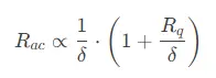
Prolonged Current Paths:
-
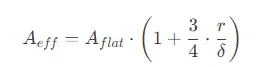
Roughness peaks/valleys (Rz=3–5μm) force current to follow contoured paths, increasing effective resistance ():
: Root-mean-square roughness.
-
II. Surface Scattering and Dielectric Coupling
-
Electromagnetic Scattering:
-
Non-specular reflections (diffuse scattering) cause phase distortion and attenuation.
-
At 28 GHz, scattering loss can exceed 30% of total insertion loss.
-
-
Dielectric Loss Enhancement:
-
Micro-voids at copper-dielectric interfaces (e.g., FR4, Rogers) localize electric fields, increasing polarization loss (higher Df).
-
III. Roughness Quantification and Loss Models
-
Hammerstad Model:
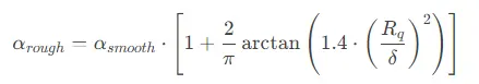
-
Modifies conductor loss based on roughness.
-
-
Huray Snowball Model:
-
Models roughness as spherical nodules (radius ) to calculate effective surface area:
-
Accurately predicts mmWave (30–100 GHz) losses.
-
IV. High-Frequency Performance Examples
| Parameter | Low Roughness (Rz=1μm) | High Roughness (Rz=5μm) |
|---|---|---|
| Insertion Loss@10 GHz | 0.5 dB/inch | 1.2 dB/inch |
| Return Loss@28 GHz | -25 dB | -18 dB |
| Phase Jitter@56 Gbps | 1.0 ps | 3.5 ps |
V. Mitigation Strategies
-
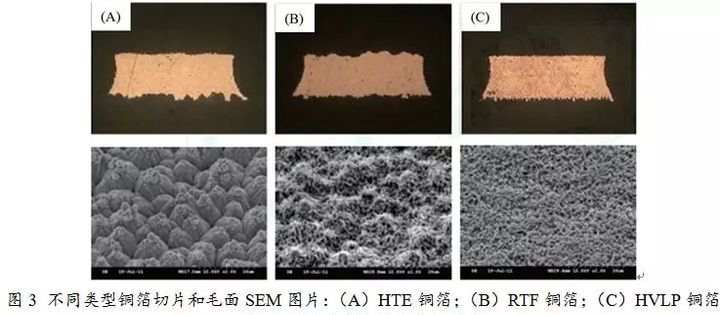
Copper Foil Selection:
-
Hyper Very Low Profile (HVLP, Rz≤1.5μm) for >10 GHz applications.
-
Reverse-Treated Foil (RTF) to minimize oxidation and roughness variation.
-
-
Surface Treatments:
-
Chemical polishing or plasma cleaning to achieve Ra≤0.3μm.
-
Smooth coatings (e.g., graphene) to fill micro-voids.
-
-
Design Compensation:
-
Pre-emphasis/equalization based on roughness models.
-
Optimize stack-up to reduce coupling between high-speed layers and rough copper.
-
VI. Validation Methods
-
Roughness Measurement:
-
White-light interferometry (3D profile, Ra/Rz).
-
Atomic force microscopy (AFM) for nanoscale resolution.
-
-
High-Frequency Testing:
-
Vector network analyzer (VNA) for S-parameters (S11/S21).
-
Time-domain reflectometry (TDR) for impedance continuity.
-
VII. Standards and Trends
-
IPC-4562A: Defines copper roughness grades (e.g., HVLP, RTF).
-
IEEE P370: Standard for high-frequency interconnect testing.
-
Trends: Nanoscale smooth copper (Rz<0.5μm) + low-Dk/Df dielectrics for 112 Gbps PAM4 and THz applications.