 PCB
PCB FPC
FPC Rigid-Flex
 FR-4
FR-4 HDI PCB
 Rogers High-Frequency Board
 PTFE Teflon High-Frequency Board
 Aluminum
 Copper Core
 PCB Assembly
 LED light PCBA
 Memory PCBA
 Power Supply PCBA
 New Energey PCBA
 Communication PCBA
 Industrial Control PCBA
 Medical Equipment PCBA
 Testing Service
 PCBA Testing Service
 Certification Application
 RoHS Certification Application
 REACH Certification Application
 CE Certification Application
 FCC Certification Application
 CQC Certification Application
 UL Certification Application
 Transformers, Inductors
 High Frequency Transformers
 Low Frequency Transformers
 High Power Transformers
 Conversion Transformers
 Sealed Transformers
 Ring Transformers
 Inductors
 Wires,Cables Customized
 Network Cables
 Power Cords
 Antenna Cables
 Coaxial Cables
 Net Position Indicator
 Solar AIS net position indicator
 Capacitors
 Connectors
 Diodes
 Embedded Processors & Controllers
 Digital Signal Processors (DSP/DSC)
 Microcontrollers (MCU/MPU/SOC)
 Programmable Logic Device(CPLD/FPGA)
 Communication Modules/IoT
 Resistors
 Through Hole Resistors
 Resistor Networks, Arrays
 Potentiometers,Variable Resistors
 Aluminum Case,Porcelain Tube Resistance
 Current Sense Resistors,Shunt Resistors
 Switches
 Transistors
 Power Modules
 Isolated Power Modules
 AC-DC Power Modules
 DC-AC Module(Inverter)
 RF and Wireless
Addressing Manufacturing Difficulties and Yield Loss Caused by Poor Design for Manufacturability in Customer Designs
2026-01-02
Design for Manufacturability (DFM) is a critICal methodology that integrates manufacturing considerations into the product design phase, ensuring that designs are not only functionally viable but also cost-effective, producible, and consistent with mass production capabilities. However, in practice, many customer designs suffer from DFM deficiencies—oversights or inconsistencies that conflict with manufacturing processes, equipment constraints, or material properties. These DFM-related issues often manifest as significant manufacturing difficulties, including prolonged setup times, frequent process failures, increased rework rates, and ultimately, substantial yield loss. Yield loss, in particular, directly impacts production costs, delivery schedules, and customer satisfaction, making the effective handling of DFM-induced manufacturing challenges a top priority for electronics manufacturing services (EMS) providers and production teams.
Poor DFM encompasses a wide range of design flaws, from overly tight dimensional tolerances and incompatible component selections to inadequate spacing between features, non-optimized PCB layouts, and insufficient consideration for assembly processes. For instance, a PCB design with minimal pad-to-pad spacing may lead to solder bridging during reflow soldering, while a component package with an unconventional footprint may require custom tooling that increases production time and error risk. These issues not only disrupt the manufacturing workflow but also reduce the proportion of usable units produced (first-pass yield), as defective products require rework or SCRapping. The root cause of such DFM gaps often lies in the customer’s design team prioritizing functional requirements over manufacturability—either due to limited manufacturing expertise, tight design timelines, or a lack of collaboration with production partners during the design phase.
Addressing manufacturing difficulties and yield loss caused by poor DFM requires a structured, collaborative approach that spans design review, issue diagnosis, cross-functional communication, design optimization, process adaptation, and long-term preventive measures. This approach must balance the need to resolve immediate production challenges with the goal of minimizing future DFM-related issues, while maintaining alignment with customer expectations and project constraints. Below is a detailed expLoRation of the key steps and strategies to effectively handle these challenges.
Proactive DFM Review: Early Identification of Potential Issues
The most effective way to mitigate DFM-induced manufacturing difficulties is to identify and address design flaws before production begins. A proactive DFM review, conducted as part of the pre-production phase, serves as the first line of defense against yield loss and process disruptions. This review should be a collaborative effort between the customer’s design team and the manufacturing partner’s engineering, production, and quality departments, leveraging specialized DFM analysis tools and manufacturing expertise.
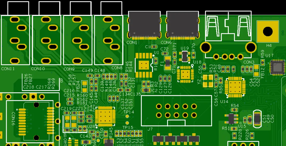
The DFM review process should focus on several critical areas to identify potential manufacturability gaps. First, PCB layout optimization: check for adequate spacing between pads, traces, and vias (to prevent short circuits and solder bridging), appropriate copper weight and trace width (to ensure reliable current carrying and heat dissipation), and optimized component placement (to facilitate assembly, reduce tooling interference, and ensure uniform reflow heating). For example, components placed too close to the edge of the PCB may cause handling issues during assembly, while uneven component distribution can lead to thermal inconsistencies during reflow soldering, resulting in solder joint defects.
Second, component selection and compatibility: verify that selected components are readily available, compatible with standard manufacturing processes (e.g., reflow vs. wave soldering temperatures), and have standardized footprints. Non-standard or obsolete components can lead to supply chain delays and require custom assembly processes, increasing the risk of errors. Additionally, ensure that component specifications (e.g., thermal tolerance, pin pitch) align with the manufacturing equipment’s capabilities—for instance, a fine-pitch QFP component (0.4mm pitch) may require high-precision placement equipment that the manufacturing line does not possess, leading to misalignment and yield loss.
Third, dimensional tolerances and geometric features: assess whether design tolerances are feasible given the manufacturing process’s capabilities. Overly tight tolerances (e.g., ±0.01mm for a PCB hole diameter) may exceed the precision of drilling equipment, resulting in non-conforming parts. Similarly, complex geometric features (e.g., sharp corners, uneven surfaces) can complicate molding or machining processes, leading to defects. The DFM review should recommend adjusting tolerances to match process capabilities or modifying geometric features to simplify production, without compromising the product’s functional performance.
To enhance the effectiveness of the DFM review, manufacturing partners should leverage specialized software tools (e.g., Mentor Graphics Xcelerator, Siemens EDA Calibre) that can automate the detection of common DFM issues, such as insufficient spacing, incorrect pad sizes, or incompatible component footprints. These tools generate detailed reports highlighting potential flaws, allowing the design and manufacturing teams to prioritize and address issues efficiently. However, automated tools should be complemented by manual review by experienced engineers, who can identify context-specific issues that may be overlooked by software (e.g., interactions between multiple design features that impact manufacturability).
Diagnosing Manufacturing Difficulties and Yield Loss Root Causes
When DFM-related issues escape the pre-production review and manifest during manufacturing, it is critical to conduct a systematic root cause analysis (RCA) to identify the specific design flaws driving the difficulties and yield loss. This RCA should be data-driven, leveraging production metrics, defect reports, and process observations to isolate the source of the problem.
First, collect and analyze production data to quantify the impact of the issues. Key metrics to consider include first-pass yield (FPY), rework rate, scrap rate, cycle time per unit, and equipment downtime. For example, a sudden drop in FPY from 95% to 70% following the introduction of a new customer design may indicate a DFM flaw. By correlating the yield drop with specific production steps (e.g., reflow soldering, component placement), the team can narrow down the potential causes—for instance, if most defects occur during reflow soldering, the issue may be related to component placement density, thermal profile incompatibility, or pad design.
Second, conduct detailed defect analysis to identify patterns. Defects such as solder bridging, tombstoning, missing components, or cracked PCBs often have distinct root causes linked to DFM. For example, tombstoning (a phenomenon where a surface-mount component stands upright on one end) is frequently caused by uneven pad sizes or asymmetrical component placement, which leads to uneven solder wetting during reflow. By examining defective units under a magnifying glass or using X-ray inspection (for hidden defects), the team can identify the specific design feature contributing to the defect.
Third, validate the root cause by conducting controlled tests. For example, if the RCA suggests that insufficient pad spacing is causing solder bridging, the team can produce a small batch of PCBs with modified pad spacing (per DFM recommendations) and compare the yield with the original design. If the modified design shows a significant improvement in yield, the root cause is confirmed. This testing phase is critical to avoid implementing unnecessary changes that may not address the core issue or could introduce new problems.
During the RCA process, it is important to involve cross-functional teams, including design engineers (customer and in-house), manufacturing engineers, process technicians, and quality analysts. Each team brings unique expertise: design engineers can explain the functional rationale behind specific design choices, while manufacturing engineers can provide insights into how those choices impact production processes. This collaboration ensures that the root cause is accurately identified and that proposed solutions balance manufacturability with functional requirements.
Cross-Functional Collaboration: Aligning Design and Manufacturing Goals
Resolving DFM-induced manufacturing difficulties requires close collaboration between the customer’s design team and the manufacturing partner, as design changes are often necessary to address the root causes. However, customers may be hesitant to modify their designs due to concerns about functional performance, project delays, or additional design costs. Therefore, effective communication and alignment of goals are critical to gaining customer buy-in for DFM improvements.
First, establish a clear communication channel between the two teams. This may involve regular meetings (in-person or virtual), shared project management tools, and direct access to key stakeholders. The manufacturing partner should present the RCA findings in a clear, data-driven manner, highlighting the impact of DFM issues on yield, cost, and delivery. For example, presenting a cost analysis showing that a 20% yield loss adds $5 per unit to production costs (due to rework and scrapping) can help the customer understand the financial implications of not addressing the design flaws.
Second, emphasize that DFM improvements are intended to preserve functional performance, not compromise it. The manufacturing partner should work with the customer’s design team to propose design modifications that address manufacturability issues while maintaining or enhancing the product’s functionality. For instance, if a PCB design’s tight trace spacing is causing short circuits, the team may recommend widening the spacing slightly or rerouting the traces—changes that do not affect the product’s electrical performance but significantly improve manufacturability.
Third, offer flexible solutions to minimize the impact on project timelines and costs. For example, if the customer is unable to make major design changes due to tight deadlines, the manufacturing partner may propose temporary process adaptations (e.g., custom tooling, adjusted thermal profiles) to mitigate the DFM issues in the short term, while working on long-term design optimizations for future production runs. This phased approach allows the customer to meet immediate delivery requirements while addressing the root cause of the yield loss.
In some cases, the manufacturing partner may need to educate the customer’s design team on DFM best practices to prevent future issues. This can involve providing DFM guidelines, conducting training sessions, or assigning a dedicated DFM engineer to collaborate with the customer during the design phase. By building the customer’s DFM expertise, the manufacturing partner reduces the likelihood of poor DFM in future designs, fostering a more collaborative and efficient relationship.
Design Optimization and Process Adaptation: Implementing Solutions
Once the root causes of DFM-induced issues are identified and customer buy-in is obtained, the next step is to implement solutions through either design optimization or process adaptation (or a combination of both). The choice between these approaches depends on the severity of the DFM flaw, the impact on functional performance, and the project constraints (timeline, cost).
Design Optimization: Addressing Root Causes at the Source
Design optimization involves modifying the customer’s design to eliminate DFM flaws, ensuring that it is compatible with standard manufacturing processes. This is the most sustainable solution, as it prevents the same issues from recurring in future production runs. Common design optimizations include:
1. PCB Layout Adjustments: Modifying pad sizes, spacing, and placement to improve solderability and reduce defects. For example, increasing pad-to-pad spacing from 0.1mm to 0.2mm can eliminate solder bridging during reflow soldering. Rerouting traces to avoid tight bends or crossings can improve signal integrity and manufacturability. Additionally, adding fiducial marks (small alignment targets) to the PCB can enhance component placement accuracy, reducing misalignment defects.
2. Component Replacement or Standardization: Replacing non-standard or obsolete components with readily available, standardized alternatives that are compatible with the manufacturing line. For example, replacing a custom-shaped connector with a standard USB connector eliminates the need for custom tooling and reduces assembly errors. Ensuring that all components have compatible thermal profiles (e.g., reflow temperature ranges) prevents component damage during soldering.
3. Tolerance and Geometric Modifications: Adjusting design tolerances to match the manufacturing process’s capabilities. For instance, relaxing the tolerance of a PCB hole diameter from ±0.01mm to ±0.02mm can improve the yield of the drilling process without affecting the fit of the component. Modifying sharp corners on a plastic part to rounded edges simplifies molding and reduces the risk of cracking.
4. Thermal and Mechanical Optimization: Ensuring that the design can withstand the thermal stresses of manufacturing processes (e.g., reflow soldering, wave soldering). For example, adding thermal relief pads (small copper connections that reduce heat transfer) to components sensitive to high temperatures prevents damage during soldering. Optimizing the mechanical structure of the product to facilitate assembly (e.g., adding alignment pins, reducing the number of fasteners) can shorten cycle time and reduce assembly errors.
After implementing design modifications, the manufacturing partner should conduct a validation test run to ensure that the changes have resolved the DFM issues. This test run should produce a small batch of units using the modified design, with detailed monitoring of yield, defect rates, and process efficiency. If the test run shows significant improvements (e.g., FPY increasing from 70% to 92%), the modified design can be adopted for full-scale production. If issues persist, further design adjustments or additional process adaptations may be necessary.
Process Adaptation: Mitigating DFM Issues in Production
In cases where design changes are not feasible (e.g., due to tight deadlines, contractual constraints), process adaptation can be used to mitigate DFM-induced manufacturing difficulties. This involves adjusting manufacturing processes, equipment settings, or tooling to accommodate the design’s flaws, without modifying the design itself. While process adaptation is a short-term solution, it can help maintain production schedules and reduce yield loss until design optimizations can be implemented.
Common process adaptations include:
1. Equipment Calibration and Customization: Adjusting the settings of manufacturing equipment to better accommodate the design’s requirements. For example, modifying the reflow soldering profile (e.g., lowering the peak temperature, extending the soak time) to prevent solder joint defects caused by incompatible component thermal tolerances. Using high-precision placement equipment (e.g., laser-guided pick-and-place machines) to handle fine-pitch components that have non-optimized footprints.
2. Custom Tooling and Fixturing: Developing custom tools or fixtures to simplify assembly and reduce errors. For example, creating a custom fixture to hold a PCB with unconventional dimensions during drilling, ensuring accurate hole placement. Using custom solder masks or stencils to control the amount of solder applied to pads with poor design (e.g., uneven pad sizes), reducing the risk of tombstoning or solder bridging.
3. Enhanced Quality Control and Inspection: Implementing additional inspection steps to catch defects early in the production process, reducing rework and scrap. For example, using automated optical inspection (AOI) after component placement to detect misalignments, or X-ray inspection to check for hidden solder joint defects in BGA components. Increasing the frequency of in-process checks (e.g., every 50 units instead of every 200 units) allows for early detection of process deviations caused by DFM issues.
4. Rework Process Optimization: Developing efficient rework procedures to address defects caused by DFM issues, reducing the time and cost of rework. For example, training technicians on specialized rework techniques for fine-pitch components with poor pad design, or using custom rework tools to minimize damage to the PCB during rework. However, it is important to note that rework should not be relied upon as a long-term solution, as it increases production costs and can compromise product reliability.
Long-Term Preventive Measures: Building a DFM-Centric Ecosystem
To minimize the recurrence of DFM-induced manufacturing difficulties and yield loss, manufacturing partners and customers should collaborate to build a DFM-centric ecosystem that integrates manufacturability considerations into every stage of the product lifecycle.
First, establish a formal DFM review process as a mandatory step in the pre-production phase. This process should be documented, with clear checklists, responsibilities, and timelines. The DFM review should be conducted early in the design phase (e.g., after the initial prototype design) to allow for timely modifications, reducing the cost and impact of changes later in the project.
Second, develop and share DFM guidelines tailored to the manufacturing partner’s capabilities. These guidelines should include specific requirements for PCB layout, component selection, tolerances, and packaging, based on the equipment, processes, and materials used by the manufacturing line. For example, if the manufacturing line uses a specific reflow soldering machine with a maximum peak temperature of 260°C, the DFM guidelines should specify that all components must have a thermal tolerance of at least 260°C.
Third, invest in DFM training and education for both internal teams and customers. Manufacturing partners should train their engineering and production teams to identify DFM issues early and communicate effectively with customers. Customers should be provided with training on DFM best practices, either through workshops, online courses, or one-on-one consultations with DFM experts. This shared expertise ensures that design teams proactively consider manufacturability from the outset.
Fourth, leverage data analytics to continuously improve DFM processes. Manufacturing partners should track and analyze DFM-related defects, yield rates, and process efficiency over time, identifying trends and areas for improvement. For example, if a particular type of DFM flaw (e.g., insufficient pad spacing) is consistently causing yield loss across multiple customer designs, the DFM guidelines can be updated to emphasize this requirement, and additional training can be provided to customers.
Fifth, foster a collaborative partnership between the customer and manufacturing partner. This involves regular communication, shared goals, and mutual respect for each other’s expertise. By treating the manufacturing partner as a strategic collaborator rather than a mere supplier, customers can leverage their manufacturing knowledge to optimize designs and avoid costly DFM issues. Conversely, manufacturing partners should prioritize understanding the customer’s functional requirements and business goals, ensuring that DFM improvements align with these objectives.
Case Study: Resolving DFM-Induced Yield Loss in a Consumer Electronics Product
To illustrate the practical application of the above strategies, consider a case where a manufacturing partner was producing a consumer electronics device (a smartwatch) for a customer, and encountered a 30% yield loss during reflow soldering. The primary defect was solder bridging between adjacent pads on the PCB, which required extensive rework and scrapping of defective units.
The RCA process began with analyzing production data, which showed that the solder bridging occurred exclusively on a section of the PCB with tight pad spacing (0.1mm) and high component density. Defect analysis under a microscope confirmed that the solder was spreading between adjacent pads during reflow, caused by insufficient spacing and uneven solder application. The manufacturing team then conducted a controlled test run with a modified PCB design, increasing the pad spacing to 0.2mm and adjusting the stencil design to control solder volume. The test run resulted in a yield improvement to 95%, confirming that the tight pad spacing was the root cause of the yield loss.
The manufacturing partner presented the RCA findings and test results to the customer’s design team, explaining the financial impact of the 30% yield loss (an additional $8 per unit in production costs) and the proposed design modifications. The customer initially expressed concerns about the impact of wider pad spacing on the PCB’s size and functional performance, but the manufacturing team collaborated with the customer’s engineers to reroute the traces and adjust component placement, ensuring that the modified design maintained the same form factor and electrical performance.
In the short term, the manufacturing partner implemented a custom stencil design to reduce solder volume, which temporarily improved the yield to 80% while the design modifications were being finalized. Once the modified design was approved, full-scale production resumed with a first-pass yield of 94%, eliminating the need for rework and reducing production costs by $7.50 per unit. To prevent future issues, the manufacturing partner provided the customer’s design team with DFM training focused on PCB layout optimization and shared a tailored DFM guideline document highlighting pad spacing requirements for their production line.
Conclusion
Manufacturing difficulties and yield loss caused by poor DFM in customer designs are significant challenges that can impact production efficiency, costs, and customer satisfaction. However, these issues are not insurmountable—they can be effectively addressed through a structured approach that includes proactive DFM reviews, systematic root cause analysis, cross-functional collaboration, targeted design optimizations or process adaptations, and long-term preventive measures.