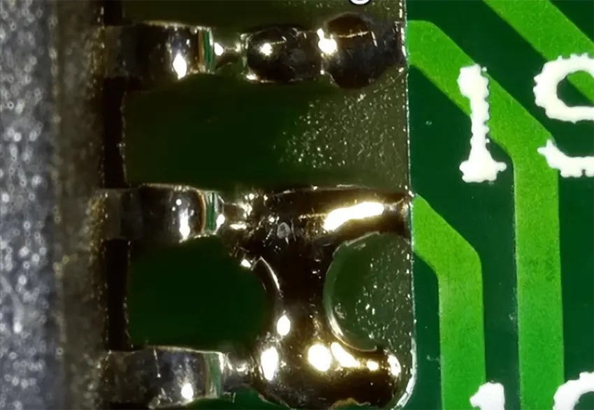
1. BasIC Understanding of Bridge DefectsBridge defect between two pins refers to a fault where solder accidentally connects adjacent pins (e.g., the two pins of a through-hole resistor or adjacent pins of a suRFace-mount IC) during soldering, resulting in an electrical short circuit. It commonly occurs in components with small pin pitches (≤2.54mm) (such as DIP-14 chips or 0805 surface-mount resistors) or due to improper manual soldering. If not repaired promptly, it can cause circuit failure (e.g., chip burnout, device shutdown). Therefore, precise manual operations are required to remove excess solder while avoiding damage to pads and pins.
Solder wick absorbs excess solder through the capillary action of copper foil. It is ideal for bridge scenarios with relatively large amounts of solder and moderate pin pitches (e.g., 1.27-2.54mm), such as bridges on through-hole Capacitor pins or edge pins of DIP chips.
- Solder Wick: Select a width that matches the pin pitch (0.8-2mm; for example, a 1mm-wide solder wick is suitable for a 1.27mm pin pitch). Priority should be given to solder wicks with a rosin coating, which eliminates the need for additional flux application and improves solder absorption efficiency.
- Temperature-Controlled Soldering Iron: Adjust to a temperature compatible with the solder’s melting point (280-320℃ for lead-free solder, 260-280℃ for leaded solder). Use a pointed tip (e.g., Type I or B) for precise contact.
- Auxiliary Tools: A 10-20x magnifying glass (for inspecting small pins), tweezers (to secure components and prevent displacement), and flux (if the wick is uncoated, apply a small amount to lower the solder’s melting point).
- Step 1: Preprocessing and Securing
Gently clamp the component body with tweezers to ensure the pins are aligned with the pads (no misalignment). If the solder at the bridge is oxidized, apply a small amount of flux to the bridged area using a cotton swab (flux removes oxidation and enhances solder fluidity). - Step 2: Positioning the Solder Wick
Lay the solder wick flat between the two bridged pins, covering the excess solder area. Ensure full contact between the wick and the pads (avoid suspension, which reduces absorption). - Step 3: Heating and Absorption with the Iron
Hold the soldering iron and press the tip lightly onto the solder wick (not directly onto the pins/pads). Heat for 3-5 seconds (until the wick discolors, the solder melts, and is absorbed). After absorption, remove the iron first, then the wick after 1-2 seconds (preventing solder reflow and re-bridging). - Step 4: Inspection and Cleaning
Inspect the bridged area with a magnifying glass. If residual solder remains, repeat Steps 2-3 (using a new section of the wick). If flux residue is left on the pads, wipe it clean with an alcohol-soaked cotton swab (to avoid PCB corrosion).
- Do not reuse the same section of the solder wick (it becomes saturated and cannot absorb more solder); cut a new section promptly.
- Do not heat a single area for more than 5 seconds (to prevent pad detachment—PCB pads typically withstand temperatures ≤350℃; prolonged heating may peel the copper foil).
- For gold-plated pins (e.g., precision connectors), avoid direct contact between the iron tip and the pins (preventing gold layer wear and reduced conductivity).
This method uses the iron tip to guide solder flow and directly separate bridged pins. It is ideal for small solder volumes and extremely fine pin pitches (≤1mm), such as bridges on QFP chip pins or 01005 components. No solder wick is required, enabling more flexible operation.
- Temperature-Controlled Soldering Iron: Use an ultra-fine pointed tip (0.2-0.5mm, e.g., WELLER LT1 tip) and set the temperature to 300-340℃ (higher temperatures ensure rapid solder melting for fine-pitch components, reducing heating time).
- Auxiliary Tools: Anti-static tweezers (insulated to avoid short circuits), toothpicks/plastic probes (non-metallic to prevent pad scratches), and a small amount of flux (to enhance solder fluidity).
- Step 1: Precise Positioning and Flux Application
Confirm the bridge location with a magnifying glass. Apply a tiny amount of flux to the gap between the two pins (only covering the bridged solder to avoid contaminating other areas). Hold the component gently with tweezers to prevent displacement during operation. - Step 2: Guided Separation with the Iron
Hold the soldering iron and insert the ultra-fine tip lightly into the bridged solder between the two pins (at a 30°-45° angle to the PCB; avoid touching the pins). Heat for 1-2 seconds (until the solder melts into a liquid). Simultaneously, use a toothpick/plastic probe to gently push the molten solder toward one pin (ensuring no residual solder remains between the pins). - Step 3: Cooling and Verification
Remove the iron and probe, then wait 2-3 seconds (for the solder to fully solidify). Use the “continuity test” function of a multimeter to check the two pins (they should be “open” normally; repeat if still “closed”).
- Do not let the iron tip touch both pins simultaneously (this causes short circuits and may burn components); always maintain “single-pin contact” or “solder-only contact.”
- Use high-temperature-resistant materials (e.g., Teflon, heat-resistant ≥260℃) for non-metallic probes to avoid melting and sticking to the solder.
- After repairing fine-pitch components (e.g., 0.5mm pitch), check for bent pins (gently straighten with tweezers to prevent re-bridging).
- Magnifying Glass/Microscope: 10-40x magnification clearly reveals small bridges (e.g., 0.2mm pitch bridges on 01005 components), avoiding blind operations.
- Anti-Static Wristband/Workbench: Discharges static electricity during repair to prevent electrostatic damage to sensitive components (e.g., CMOS chips).
- Solder Sucker (Backup): If the wick fails to absorb thoroughly, use a solder sucker to remove residual solder (suitable for large bridges on through-hole components).
- Mistake 1: Excessively High Iron Temperature (>350℃)
Consequence: Pad detachment, pin oxidation. Mitigation: Adjust the temperature based on solder type (lead-free/leaded) and component material (plastic/metal packaging); do not exceed 340℃. - Mistake 2: Operating Without Flux
Consequence: Poor solder fluidity, difficult removal, and pad scratches. Mitigation: Apply a small amount of flux regardless of whether the wick is coated (especially for oxidized old solder). - Mistake 3: Fast/Forceful Operation
Consequence: Bent pins, pad peeling. Mitigation: Perform each step slowly and steadily; apply light pressure and movement with the iron and probe to avoid external force.
The key to repairing pin bridges is “temperature control, precision, and gentle operation”:
- Temperature control is fundamental: Adjust the iron temperature based on solder and component type to avoid high-temperature damage.
- Precision positioning is a prerequisite: Use a magnifying glass to identify the bridge range; do not heat blindly.
- Gentle operation is critical: Whether using solder wick or iron separation, minimize external impact on pads and pins.
After repair, verify success through “visual inspection (no residual solder)” and “continuity test (open pins)” to ensure complete bridge removal without secondary damage, ultimately restoring normal circuit function.
 PCB
PCB FPC
FPC Rigid-Flex
 FR-4
FR-4 HDI PCB
 Rogers High-Frequency Board
 PTFE Teflon High-Frequency Board
 Aluminum
 Copper Core
 PCB Assembly
 LED light PCBA
 Memory PCBA
 Power Supply PCBA
 New Energey PCBA
 Communication PCBA
 Industrial Control PCBA
 Medical Equipment PCBA
 Testing Service
 PCBA Testing Service
 Certification Application
 RoHS Certification Application
 REACH Certification Application
 CE Certification Application
 FCC Certification Application
 CQC Certification Application
 UL Certification Application
 Transformers, Inductors
 High Frequency Transformers
 Low Frequency Transformers
 High Power Transformers
 Conversion Transformers
 Sealed Transformers
 Ring Transformers
 Inductors
 Wires,Cables Customized
 Network Cables
 Power Cords
 Antenna Cables
 Coaxial Cables
 Net Position Indicator
 Solar AIS net position indicator
 Capacitors
 Connectors
 Diodes
 Embedded Processors & Controllers
 Digital Signal Processors (DSP/DSC)
 Microcontrollers (MCU/MPU/SOC)
 Programmable Logic Device(CPLD/FPGA)
 Communication Modules/IoT
 Resistors
 Through Hole Resistors
 Resistor Networks, Arrays
 Potentiometers,Variable Resistors
 Aluminum Case,Porcelain Tube Resistance
 Current Sense Resistors,Shunt Resistors
 Switches
 Transistors
 Power Modules
 Isolated Power Modules
 AC-DC Power Modules
 DC-AC Module(Inverter)
 RF and Wireless