 PCB
PCB FPC
FPC Rigid-Flex
 FR-4
FR-4 HDI PCB
 Rogers High-Frequency Board
 PTFE Teflon High-Frequency Board
 Aluminum
 Copper Core
 PCB Assembly
 LED light PCBA
 Memory PCBA
 Power Supply PCBA
 New Energey PCBA
 Communication PCBA
 Industrial Control PCBA
 Medical Equipment PCBA
 Testing Service
 PCBA Testing Service
 Certification Application
 RoHS Certification Application
 REACH Certification Application
 CE Certification Application
 FCC Certification Application
 CQC Certification Application
 UL Certification Application
 Transformers, Inductors
 High Frequency Transformers
 Low Frequency Transformers
 High Power Transformers
 Conversion Transformers
 Sealed Transformers
 Ring Transformers
 Inductors
 Wires,Cables Customized
 Network Cables
 Power Cords
 Antenna Cables
 Coaxial Cables
 Net Position Indicator
 Solar AIS net position indicator
 Capacitors
 Connectors
 Diodes
 Embedded Processors & Controllers
 Digital Signal Processors (DSP/DSC)
 Microcontrollers (MCU/MPU/SOC)
 Programmable Logic Device(CPLD/FPGA)
 Communication Modules/IoT
 Resistors
 Through Hole Resistors
 Resistor Networks, Arrays
 Potentiometers,Variable Resistors
 Aluminum Case,Porcelain Tube Resistance
 Current Sense Resistors,Shunt Resistors
 Switches
 Transistors
 Power Modules
 Isolated Power Modules
 AC-DC Power Modules
 DC-AC Module(Inverter)
 RF and Wireless
Mandatory Visual Inspection Items for PCBA Post-Assembly
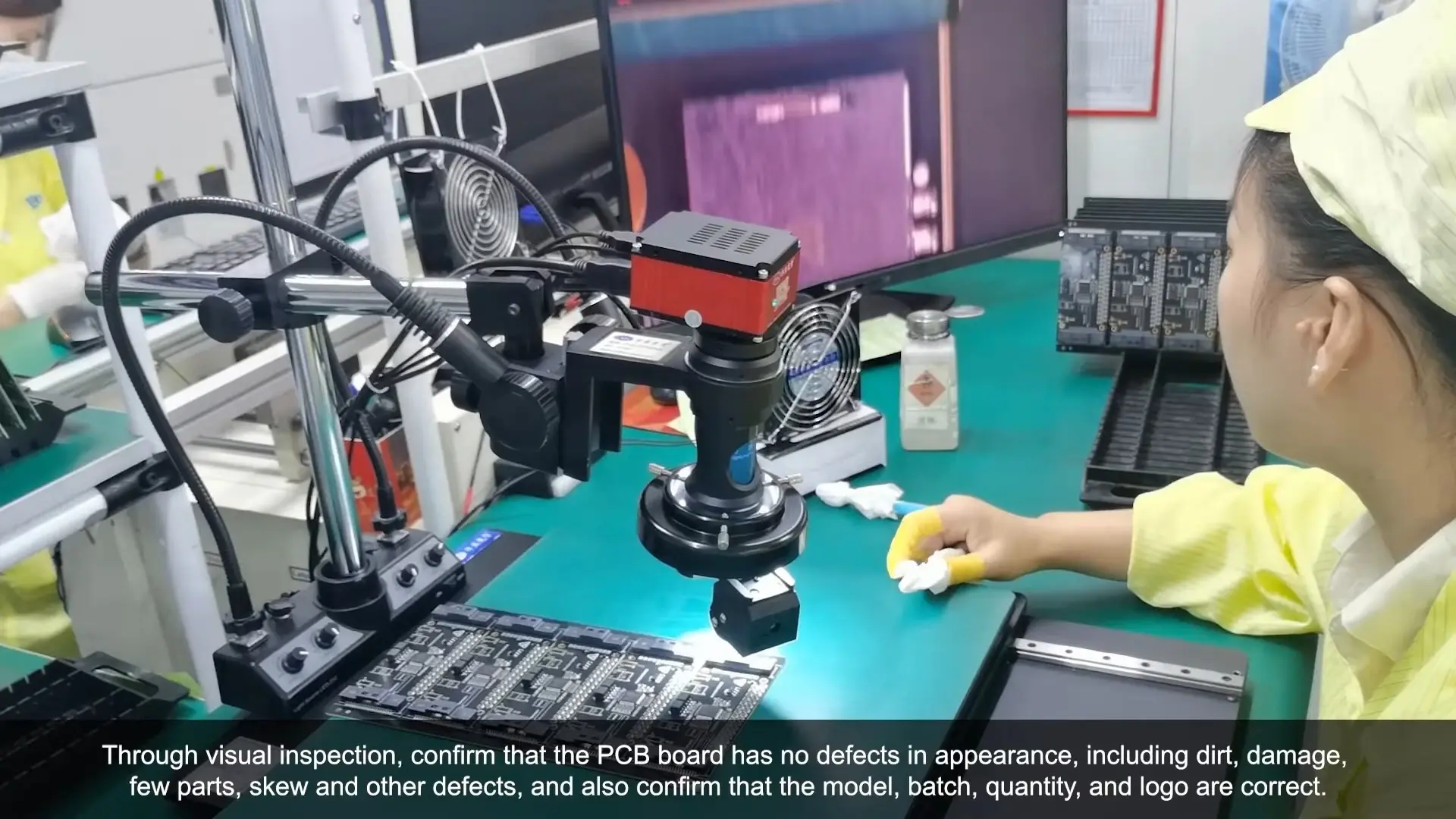
Abstract: Visual inspection of PCBA is critICal for soldering quality and reliability. Per IPC-A-610 standards, key mandatory items include missing components, misalignment, solder bridging, reversed polarity, and physical damage, directly impacting electrical peRFormance and product longevity.
1. Missing Components
-
Inspection Focus:
-
Verify all placement locations against BOM, especially miniature components (e.g., 0201 Resistors, 0402 capacitors) and bottom-terminated devices (QFN, LGA).
-
-
Acceptance Criteria:
-
Zero tolerance: Any missing component at designed locations fails inspection (IPC-A-610 Class 2/3).
-
-
Tools:
-
AOI (Automated Optical Inspection) with >99.5% detection rate, paired with barcode traceability.
-
2. Component Misalignment
-
Tolerance Standards (relative to pads):
Component Max. Allowable Offset Visual Reference Chip Components ≤25% pad width Exposed copper ≤1/4 component width IC/SOP ≤50% lead width 100% lead coverage on pad BGA ≤15% ball diameter Ball-to-pad center offset ≤0.05mm -
Failure Impact:
-
Offset >25% reduces solder joint strength by 40% and cuts thermal cycle life by 5×.
-
3. Solder Bridging
-
High-Risk Areas:
-
Fine-pitch IC leads (pitch ≤0.5mm), QFN side wings, adjacent BGA balls.
-
-
Acceptance Criteria:
-
Class 2/3: Reject any visible solder connection between pins (IPC-A-610 5.2.5).
-
Exemption: Designed thermal bridges (must be documented).
-
-
Rework:
-
Hot air gun + solder wick, localized temperature ≤300℃/5 sec.
-
4. Reversed Polarity
-
Critical Components:
-
Electrolytic capacitors, diodes, LEDs, ICs (marking orientation).
-
-
Inspection Method:
-
Match silkscreen polarity symbols (+/-/◁) with component markings.
-
Chip orientation: U1/U2 reference corner aligns with IC dot/notch.
-
-
Risk Level:
-
90% explosion rate upon power-up; classified as critical defect.
-
5. Physical Damage
-
Inspection Items:
Damage Type Rejection Criteria Tools Component Crack Visible cracks in ceramics/magnetics 20× magnifier PCB Scratch Exposed copper >50% depth or >3mm length Macro camera + ruler Lead Deformation Coplanarity >0.1mm (IPC-A-610 8.2.4) Laser confocal microscope -
Root Cause:
-
60% damage from pick-and-place nozzle overload or depaneling stress.
-
6. Other Mandatory Items
-
Solder Balling:
-
Remove balls >0.13mm diameter or <0.13mm apart (IPC-A-610 5.3.11).
-
-
Cold Solder:
-
Solder wetting angle >90° or no fillet at lead edges (per IPC-J-STD-001).
-
-
Foreign Material:
-
Zero tolerance for conductive debris; fiber residue ≤5mm².
-
Inspection Process Optimization
-
AOI Programming:
-
Layered strategy: Global scan for missing/misaligned parts → local high-mag check for bridges/cold solder.
-
-
Manual Review:
-
45° angled lighting for hidden BGA bridges; X-ray verification (↑90% cold solder detection).
-
-
Data Traceability:
-
Link AOI images to serial numbers; implement SPC charts for defects (CPK≥1.33).
-
Conclusion
PCBA visual inspection must enforce the "Three No's Principle":
-
No acceptance of defects (zero tolerance for polarity reversal/bridging)
-
No creation of defects (error-proof process design)
-
No passing of defects (100% AOI + manual review for critical areas)
Implement tiered controls per IPC standards with high-precision AOI (5μm resolution) and failure analysis tools to ensure defect escape rate <200 ppm.