 PCB
PCB FPC
FPC Rigid-Flex
 FR-4
FR-4 HDI PCB
 Rogers High-Frequency Board
 PTFE Teflon High-Frequency Board
 Aluminum
 Copper Core
 PCB Assembly
 LED light PCBA
 Memory PCBA
 Power Supply PCBA
 New Energey PCBA
 Communication PCBA
 Industrial Control PCBA
 Medical Equipment PCBA
 Testing Service
 PCBA Testing Service
 Certification Application
 RoHS Certification Application
 REACH Certification Application
 CE Certification Application
 FCC Certification Application
 CQC Certification Application
 UL Certification Application
 Transformers, Inductors
 High Frequency Transformers
 Low Frequency Transformers
 High Power Transformers
 Conversion Transformers
 Sealed Transformers
 Ring Transformers
 Inductors
 Wires,Cables Customized
 Network Cables
 Power Cords
 Antenna Cables
 Coaxial Cables
 Net Position Indicator
 Solar AIS net position indicator
 Capacitors
 Connectors
 Diodes
 Embedded Processors & Controllers
 Digital Signal Processors (DSP/DSC)
 Microcontrollers (MCU/MPU/SOC)
 Programmable Logic Device(CPLD/FPGA)
 Communication Modules/IoT
 Resistors
 Through Hole Resistors
 Resistor Networks, Arrays
 Potentiometers,Variable Resistors
 Aluminum Case,Porcelain Tube Resistance
 Current Sense Resistors,Shunt Resistors
 Switches
 Transistors
 Power Modules
 Isolated Power Modules
 AC-DC Power Modules
 DC-AC Module(Inverter)
 RF and Wireless
Laser-to-PCB Waveguide Optical Axis Alignment Calibration in Optical Module Assembly

The critical challenge in assembling high-speed optical modules (e.g., 400G/800G) lies in achieving sub-micron optical axis alignment between laser diodes (LDs) and PCB-embedded waveguides. Axial misalignment exceeding ±0.5μm causes significant coupling loss (>3dB), degrading transmission peRFormance.
1. Fundamentals of Optical Axis Alignment
1.1 Coupling Efficiency Model
Coupling efficiency (η) between LD and waveguide depends on mode-field matching:
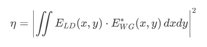
Lateral offsets (Δx, Δy) are most critical, with ~1.2dB loss per 1μm misalignment.
1.2 Alignment Degrees of Freedom
Six parameters require calibration (Figure 1):
-
Positional: X/Y/Z translation (±0.1μm accuracy);
-
Angular: θx (pitch), θy (yaw), θz (roll) (±0.05° accuracy).
2. Calibration Equipment and Procedures
2.1 Active Alignment System
-
Key components:
-
Six-axis nano-positioning stage (0.01μm resolution);
-
IR vision system (1310/1550nm, 1000× magnification);
-
Real-time power monitor (10kHz sampling).
-
-
Procedure:
-
Coarse alignment: Machine vision locates waveguide facet (<5μm error);
-
Fine alignment: Hill-climbing algorithm optimizes parameters using power feedback;
-
Locking: UV curing with 2-3μm pre-offset compensation.
-
2.2 Passive Alignment Technology
-
Applications: Cost-effective mass production;
-
Techniques:
-
Silicon V-grooves with mechanical stops (±1μm accuracy);
-
Flip-chip self-alignment via solder surface tension (±0.8μm correction).
-
3. Thermal Expansion Compensation
3.1 Thermal Drift Model
Axial shift (ΔL) due to temperature change (ΔT):
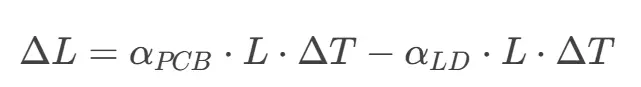
CTE mismatch (αPCB≈14ppm/℃ for FR-4 vs. αLD≈4.5ppm/℃ for InP) causes thermal drift.
3.2 Compensation Strategies
-
Material matching: Use low-CTE substrates (e.g., ceramic, 6ppm/℃);
-
Structural design:
-
Symmetric LD/waveguide layout;
-
Compliant hinges to absorb deformation;
-
-
Dynamic control: TEC with closed-loop feedback (±0.1℃ stability).
4. Validation and Testing
4.1 Alignment Accuracy Tests
-
Near-field scanning: IR camera measures spot-to-waveguide core deviation (Figure 2);
-
IL/RL tests: Insertion loss ≤1.5dB, return loss ≥40dB.
4.2 Reliability Verification
-
Temperature cycling: -40℃~+85℃ for 500 cycles, <0.3dB loss variation;
-
Vibration testing: GR-468-compliant random vibration (20Hz-2000Hz), <0.2μm shift.
5. Case Study: 400G QSFP-DD Module
-
LD type: EML, 1310nm;
-
Waveguide: SiPh embedded waveguide, 3μm mode diameter;
-
Results: 92% coupling efficiency post-alignment, 0.15μm shift after thermal cycling.