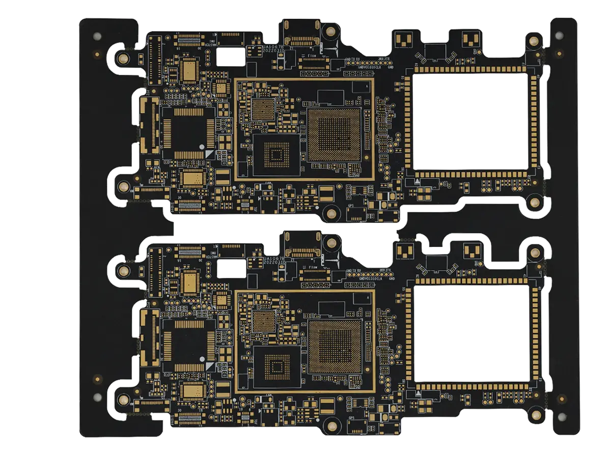
 PCB
PCB FPC
FPC Rigid-Flex
 FR-4
FR-4 HDI PCB
 Rogers High-Frequency Board
 PTFE Teflon High-Frequency Board
 Aluminum
 Copper Core
 PCB Assembly
 LED light PCBA
 Memory PCBA
 Power Supply PCBA
 New Energey PCBA
 Communication PCBA
 Industrial Control PCBA
 Medical Equipment PCBA
 Testing Service
 PCBA Testing Service
 Certification Application
 RoHS Certification Application
 REACH Certification Application
 CE Certification Application
 FCC Certification Application
 CQC Certification Application
 UL Certification Application
 Transformers, Inductors
 High Frequency Transformers
 Low Frequency Transformers
 High Power Transformers
 Conversion Transformers
 Sealed Transformers
 Ring Transformers
 Inductors
 Wires,Cables Customized
 Network Cables
 Power Cords
 Antenna Cables
 Coaxial Cables
 Net Position Indicator
 Solar AIS net position indicator
 Capacitors
 Connectors
 Diodes
 Embedded Processors & Controllers
 Digital Signal Processors (DSP/DSC)
 Microcontrollers (MCU/MPU/SOC)
 Programmable Logic Device(CPLD/FPGA)
 Communication Modules/IoT
 Resistors
 Through Hole Resistors
 Resistor Networks, Arrays
 Potentiometers,Variable Resistors
 Aluminum Case,Porcelain Tube Resistance
 Current Sense Resistors,Shunt Resistors
 Switches
 Transistors
 Power Modules
 Isolated Power Modules
 AC-DC Power Modules
 DC-AC Module(Inverter)
 RF and Wireless
Key Technologies for Interlayer Alignment Accuracy Control in Blind/Buried Via PCBs
Key Technologies for Interlayer Alignment Accuracy Control in Blind/Buried Via PCBs
Interlayer alignment accuracy in blind/buried via PCBs is critICal for ensuring the reliability of high-density interconnect (HDI) boards. Misalignment can lead to signal integrity degradation, impedance mismatch, and reliability risks (e.g., CAF failure). This article systematically details key technologies from material, process, equipment, and inspection perspectives.
I. Material Selection and Thermal Matching
-
Low-CTE Substrates
-
High-stability materials (e.g., MEGTRON 6, IT-180A) with Tg ≥170℃ and CTE ≤14 ppm/℃ minimize thermal deformation during lamination and reflow.
-
CTE difference between core and prepreg must be ≤3 ppm/℃ to prevent interlayer stress.
-
-
Copper Foil Optimization
-
Reverse-treated foil (RTF) or hyper very low-profile foil (HVLP) with suRFace roughness Rz ≤3μm reduces dimensional fluctuations during pattern transfer.
-
II. High-Precision Pattern Alignment
-
Laser Direct Imaging (LDI)
-
Achieves ≤5μm alignment accuracy using UV lasers (355nm), eliminating film expansion errors.
-
Dynamic focus compensation (DFC) corrects local warpage-induced distortions.
-
-
Inner Layer Fiducial Design
-
≥4 global and local fiducials per layer, spaced ≥100mm, with cross/concentric structures for reliable recognition.
-
X-ray alignment systems (e.g., Orbotech XBOLT) enable sub-micron alignment of buried vias and inner traces.
-
III. Precision Drilling and Via Filling
-
Laser Drilling Optimization
-
UV picosecond lasers (10ps pulse width) create blind vias with ≤3° taper and Ra ≤5μm wall roughness.
-
Energy density gradient control (e.g., 1.2J/cm² at entrance vs. 0.8J/cm² at exit) suppresses "nail head" effects.
-
-
Via Filling Uniformity
-
Pulse reverse plating (PRP): 2ASD forward/0.5ASD reverse current achieves ≤10% dimple depth.
-
Plasma activation (O₂/N₂ mix) pre-treatment enhances copper adhesion.
-
IV. Lamination Process Control
-
Staged Pressure & Temperature Profile
-
Initial 0.5MPa pressure (prevents slippage) → 1.5MPa at Tg+20℃ → Constant-pressure curing.
-
Ramp rates ≤2℃/min (heating) and ≤3℃/min (cooling) minimize thermal stress.
-
-
Vacuum-Assisted Lamination
-
≤50Pa vacuum with 1.5mm silicone cushions ensures ≥95% pressure uniformity.
-
V. Intelligent Inspection & Feedback
-
Real-Time Warpage Monitoring
-
Laser interferometers measure post-lamination warpage (target ≤0.1% thickness), feeding data to drilling machines for positional compensation.
-
-
Interlayer Alignment Analysis
-
Cross-sectioning + metallurgical microscopy: Measures via offset (target ≤±15μm).
-
3D X-ray CT: Reconstructs via structures to analyze misalignment modes.
-
VI. Typical Process Parameters
| Process Step | Key Parameter | Target Value |
|---|---|---|
| Laser Alignment | X/Y Repeatability | ≤±3μm |
| Lamination Uniformity | Intra-board Temperature Variation | ≤±2℃ |
| Blind Via Position | vs. Design Coordinates | ≤±10μm |
| Plating Uniformity | Entrance vs. Center Thickness | ≤15% Difference |