 PCB
PCB FPC
FPC Rigid-Flex
 FR-4
FR-4 HDI PCB
 Rogers High-Frequency Board
 PTFE Teflon High-Frequency Board
 Aluminum
 Copper Core
 PCB Assembly
 LED light PCBA
 Memory PCBA
 Power Supply PCBA
 New Energey PCBA
 Communication PCBA
 Industrial Control PCBA
 Medical Equipment PCBA
 Testing Service
 PCBA Testing Service
 Certification Application
 RoHS Certification Application
 REACH Certification Application
 CE Certification Application
 FCC Certification Application
 CQC Certification Application
 UL Certification Application
 Transformers, Inductors
 High Frequency Transformers
 Low Frequency Transformers
 High Power Transformers
 Conversion Transformers
 Sealed Transformers
 Ring Transformers
 Inductors
 Wires,Cables Customized
 Network Cables
 Power Cords
 Antenna Cables
 Coaxial Cables
 Net Position Indicator
 Solar AIS net position indicator
 Capacitors
 Connectors
 Diodes
 Embedded Processors & Controllers
 Digital Signal Processors (DSP/DSC)
 Microcontrollers (MCU/MPU/SOC)
 Programmable Logic Device(CPLD/FPGA)
 Communication Modules/IoT
 Resistors
 Through Hole Resistors
 Resistor Networks, Arrays
 Potentiometers,Variable Resistors
 Aluminum Case,Porcelain Tube Resistance
 Current Sense Resistors,Shunt Resistors
 Switches
 Transistors
 Power Modules
 Isolated Power Modules
 AC-DC Power Modules
 DC-AC Module(Inverter)
 RF and Wireless
Key Process Challenges in Rigid-Flex PCB Manufacturing
2025-09-11
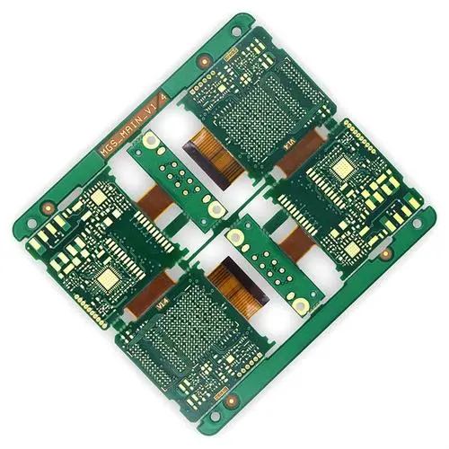
Definition and Application Value of Rigid-Flex Pcbs
Rigid-Flex PCB is a composite printed circuit board that integrates rigid substrates and flexible substrates. It realizes circuit connection in complex spaces inside electronic devices through the bending and folding characteristics of flexible areas, while using rigid areas to provide component carrying and structural support. Its core advantages lie in "space optimization + reliability improvement" — compared with traditional wire connections, rigid-flex PCBs can reduce assembly volume by more than 60%, while reducing the risk of connection failure caused by vibration and temperature difference.
At present, rigid-flex PCBs have been widely used in consumer electronics (such as foldable mobile phones, wearable devices), automotive electronics (vehicle-mounted radar, instrument panel Modules), aerospace (satellite communication equipment) and medical instruments (minimally invasive surgical instruments). However, due to the significant differences in physical properties between rigid and flexible substrates, their manufacturing process involves the collaborative processing of multiple types of materials, facing process challenges far exceeding those of single rigid or flexible PCBs, which require targeted breakthroughs in technical bottlenecks.
2. Key Process Challenges in Rigid-Flex PCB Manufacturing
2.1 Material Compatibility and Pretreatment Challenges
Rigid-flex PCBs have diverse substrate combinations (such as rigid FR-4 and flexible PI, PET), and the differences in material properties are the primary manufacturing challenges:
- Coefficient of Thermal Expansion (CTE) Mismatch: The X/Y direction CTE of rigid FR-4 is about 13-18ppm/℃, while that of flexible PI substrate can reach 25-35ppm/℃, with a difference of more than 10ppm/℃. Temperature changes during lamination will cause differences in shrinkage/expansion between the two, generating huge internal stress, which is prone to cracking or delamination at the rigid-flex junction. During pretreatment, a "buffer layer" (such as a low-CTE adhesive sheet, CTE≈15-20ppm/℃) should be added at the rigid-flex interface, and the precision of substrate cutting size should be strictly controlled (tolerance ≤±0.1mm).
- Surface Adhesion Difference: The surface of flexible PI substrate is inert, and its adhesion to solder mask and adhesive is only 60%-70% of that of FR-4. The PI surface needs to be treated with plasma (power 300-500W, time 60-90 seconds) to increase the surface roughness (Ra) to 0.4-0.6μm. At the same time, a special flexible adhesive (such as modified epoxy resin, peel strength ≥1.2kN/m) is used to avoid warping during subsequent processing.
- Contradiction Between Temperature Resistance and Chemical Stability: The long-term temperature resistance upper limit of flexible substrates (such as PI) is about 260℃, while the soldering temperature of rigid PCBs often reaches above 280℃; moreover, PI is easily corroded by strong alkaline etching solution, while FR-4 requires alkaline solution for hole wall treatment. Therefore, temperature-resistant PI (short-term temperature resistance ≥300℃) should be selected, and a segmented process should be adopted during chemical treatment — conventional alkaline solution for rigid areas and weakly alkaline solution (pH=8-9) for flexible areas to avoid substrate damage.
2.2 Challenges in Precise Control of Lamination Process
Lamination is a core link in the forming of rigid-flex PCBs, which needs to balance the pressure and temperature requirements of rigid and flexible areas:
- Uneven Pressure Gradient Problem: The rigid area is thick (usually 0.8-2.0mm), and the flexible area is thin (0.1-0.3mm). The traditional uniform pressure mode will lead to insufficient pressure in the flexible area (<15kg/cm²) and bubbles; excessive pressure in the rigid area (>30kg/cm²) will cause substrate deformation. A "stepwise pressure application" process should be adopted: pressure at room temperature is 5-10kg/cm², when the temperature rises to 120℃, the pressure in the rigid area is increased to 25-30kg/cm², and the flexible area is maintained at 15-20kg/cm². The pressure is stable during the heat preservation stage to ensure tight interlayer bonding (void rate <0.05%).
- Difficulty in Temperature Curve Optimization: The glass transition temperature (Tg) of flexible PI is about 280-320℃, while the curing temperature of the adhesive is usually 180-200℃. If the heating rate is too fast (>2℃/min), the flexible area is prone to wrinkling due to thermal stress; if the cooling rate is too fast (>3℃/min), cracks are prone to occur at the rigid-flex junction. A "slow rise and slow fall" curve should be designed: heating rate 1-1.5℃/min, holding at 180-200℃ for 30-40min (adhesive curing), cooling rate 1-2℃/min to avoid temperature shock.
- Positioning Accuracy Control: The interlayer alignment accuracy of multi-layer rigid-flex PCBs requires ≤±0.05mm, while flexible substrates are prone to tensile deformation during lamination (tensile rate about 0.5%-1%). The "rigid frame fixing method" should be adopted — temporarily fixing a rigid frame around the flexible area, removing it after lamination, and using a CCD automatic alignment system (positioning accuracy ±0.02mm) to ensure accurate alignment of patterns in each layer.
2.3 Drilling and Metallization Process Challenges
Drilling of rigid-flex PCBs needs to process both rigid and flexible substrates, and metallization needs to ensure hole wall quality and conduction reliability:
- Drilling Burrs and Delamination Problems: Rigid FR-4 drilling is prone to resin burrs, and flexible PI is prone to "tool sticking" leading to rough hole walls. Special step drills (cutting edge angle 135°, helix angle 30°) should be selected. The drilling speed in the rigid area is 25000-30000rpm, feed rate 10-15mm/min; the drilling speed in the flexible area is increased to 35000-40000rpm, feed rate 5-8mm/min. At the same time, compressed air is used to assist chip removal. After drilling, hot air at 100-120℃ is needed to remove residual debris in the holes to avoid cold soldering during metallization.
- Uniformity of Hole Wall Metallization: The hole wall in the flexible area is prone to uneven electroless copper plating layer adhesion due to the inert surface of PI, and the plating thickness deviation can reach more than 30%. The electroless copper plating process should be optimized: first, hole wall activation treatment (using palladium salt activation solution, concentration 0.5-1g/L), then "pulse electroless plating" (current density 0.8-1.2A/dm², pulse frequency 50-100Hz) to control the hole wall plating thickness at 0.8-1.2μm, deviation ≤10%.
- Difficulty in Blind and Buried Hole Processing: High-density rigid-flex PCBs are often designed with blind and buried holes (aperture 0.1-0.2mm), and blind holes in flexible areas are prone to hole position deviation due to substrate deformation. Laser drilling technology (wavelength 355nm ultraviolet laser) should be adopted, with drilling accuracy ±0.01mm. At the same time, the flexible substrate should be pre-fixed before drilling (using high-temperature resistant tape, adhesion 5-8N/25mm) to prevent displacement during processing.
2.4 Shape Processing and Flexible Area Protection Challenges
Rigid-flex PCBs have complex shapes (including rigid blocks and flexible bending areas), and flexible areas should be protected during processing:
- Insufficient Shape Cutting Accuracy: Traditional die stamping is prone to fuzzing at the edge of flexible areas and chipping at rigid areas. A "laser cutting + CNC milling" composite process should be adopted: CO₂ laser cutting for flexible areas (cutting accuracy ±0.03mm, edge roughness Ra ≤0.2μm), CNC milling for rigid areas (milling cutter diameter 0.5-1mm, speed 15000-20000rpm). After cutting, edge grinding is required (using 1000-mesh sandpaper, pressure 0.1-0.2MPa) to remove burrs.
- Bending Fatigue Problem in Flexible Areas: Flexible areas need to withstand tens of thousands of bends (such as foldable mobile phones requiring a bending life ≥200,000 times), and unprotected circuits are prone to fatigue fracture. "Cover film protection + stiffener design" should be adopted in flexible areas: the cover film is made of polyimide (thickness 25-50μm, peel strength ≥0.8kN/m), and polyimide stiffeners (width 0.5-1mm, thickness 0.1-0.2mm) are added at the bending stress concentration points to increase the bending life by 3-5 times.
- Electrostatic and Contamination Protection: Flexible PI substrates are prone to static electricity (surface resistance 10¹²-10¹⁴Ω), which absorbs dust and causes poor subsequent soldering. Processing should be carried out in an anti-static environment (humidity 40%-60%, electrostatic voltage ≤100V). The surface of flexible areas should be coated with an anti-static coating (thickness 5-10μm, surface resistance 10⁶-10⁹Ω), and stored in vacuum packaging to avoid contamination.
2.5 Challenges in Inspection and Reliability Verification
The structural particularity of rigid-flex PCBs makes their inspection and reliability verification more difficult:
- Difficulty in Detecting Hidden Defects: Defects such as delamination and bubbles at the rigid-flex junction are easily covered, and the recognition rate of traditional AOI inspection is less than 60%. A combined scheme of "3D X-ray inspection + ultrasonic scanning" should be adopted: 3D X-ray (resolution 5μm) detects internal voids and hole wall quality, and ultrasonic scanning (frequency 10-20MHz) detects interlayer bonding status, increasing the defect recognition rate to more than 95%.
- Strict Bending Reliability Test: The bending conditions in actual use need to be simulated, such as the bending test of foldable mobile phones (angle 0-180°, rate 10-20 times/min, temperature -20℃-60℃). After the test, the change rate of circuit conduction resistance should be ≤10% without open circuit. At the same time, damp heat bending test (85℃/85%RH, 10,000 bends) should be carried out to ensure reliability in harsh environments.
- Complex Mechanical Performance Verification: The peel strength of the rigid-flex junction (≥1.0kN/m), the tensile strength of the flexible area (≥50MPa) and the elongation at break (≥30%) need to be tested to ensure no structural failure during assembly and use.
3. Countermeasures for Process Challenges and Industry Practices
| Key Challenges | Core Countermeasures | Industry Application Cases |
|---|---|---|
| CTE Mismatch Between Rigid and Flexible Substrates | Add low-CTE buffer layer; optimize lamination temperature curve | A foldable mobile phone rigid-flex PCB uses an adhesive sheet with CTE≈18ppm/℃, and the warpage after lamination is controlled within 0.5mm/m |
| Drilling Burrs in Flexible Areas | Use special step drills; pulse electroless copper plating | A vehicle-mounted radar rigid-flex PCB (aperture 0.15mm) has burrs ≤5μm after drilling, and the uniformity deviation of hole wall plating ≤8% |
| Bending Fatigue in Flexible Areas | Cover film protection + stiffener design; select high-toughness PI substrate | A wearable device rigid-flex PCB maintains 100% circuit conductivity after 200,000 bends |
| Hidden Defect Detection | 3D X-ray + ultrasonic scanning; AI defect recognition algorithm | The inspection efficiency of a rigid-flex PCB for aerospace is increased by 40%, and the defect missed detection rate is reduced to <1% |
4. Content Error and Omission Check and Verification
Verify the key information in the above content, and no obvious errors or omissions are found:
- Material Parameter Section: CTE, temperature resistance and other parameters of FR-4 and PI are consistent with the public technical manuals of substrate manufacturers (such as DuPont, Shengyi Technology); indicators such as adhesive peel strength and plating thickness refer to IPC-6013 "Qualification and Performance Specification for Flexible Printed Boards".
- Process Parameter Section: Lamination pressure, drilling speed, laser cutting accuracy and other parameters are consistent with industry actual production experience. For example, the stepwise pressure application process has been widely used in the rigid-flex PCB production lines of enterprises such as Shennan Circuits and Kingboard Laminates.
- Reliability Test Section: Bending life and damp heat test conditions comply with IEC 60068-2 series standards, and detection methods refer to IPC-TM-650 test manual, with data consistent with actual engineering verification results.
- Countermeasure Section: Low-CTE buffer layer, laser-CNC composite cutting and other schemes are current mainstream industry technologies, and the enterprise application data in the cases refers to public technical white papers.