 PCB
PCB FPC
FPC Rigid-Flex
 FR-4
FR-4 HDI PCB
 Rogers High-Frequency Board
 PTFE Teflon High-Frequency Board
 Aluminum
 Copper Core
 PCB Assembly
 LED light PCBA
 Memory PCBA
 Power Supply PCBA
 New Energey PCBA
 Communication PCBA
 Industrial Control PCBA
 Medical Equipment PCBA
 Testing Service
 PCBA Testing Service
 Certification Application
 RoHS Certification Application
 REACH Certification Application
 CE Certification Application
 FCC Certification Application
 CQC Certification Application
 UL Certification Application
 Transformers, Inductors
 High Frequency Transformers
 Low Frequency Transformers
 High Power Transformers
 Conversion Transformers
 Sealed Transformers
 Ring Transformers
 Inductors
 Wires,Cables Customized
 Network Cables
 Power Cords
 Antenna Cables
 Coaxial Cables
 Net Position Indicator
 Solar AIS net position indicator
 Capacitors
 Connectors
 Diodes
 Embedded Processors & Controllers
 Digital Signal Processors (DSP/DSC)
 Microcontrollers (MCU/MPU/SOC)
 Programmable Logic Device(CPLD/FPGA)
 Communication Modules/IoT
 Resistors
 Through Hole Resistors
 Resistor Networks, Arrays
 Potentiometers,Variable Resistors
 Aluminum Case,Porcelain Tube Resistance
 Current Sense Resistors,Shunt Resistors
 Switches
 Transistors
 Power Modules
 Isolated Power Modules
 AC-DC Power Modules
 DC-AC Module(Inverter)
 RF and Wireless
Key Points of Process Control in SMT Solder Paste Printing Process
2025-03-15
I. Solder Paste Usage Control
- Follow the first - in - first - out principle. After the solder paste arrives at the factory, immediately affix the "Solder Paste Usage Control Label" and store it in a refrigerator at 2 - 8°C. Use the solder paste according to the expiration date in sequence. Take the solder paste with a smaller number first. Let the solder paste warm up in a moisture - proof box for more than 4 hours before use. Fill in the solder paste control form when taking the solder paste.
II. Refrigerator Temperature Control
- The refrigerator temperature should be maintained at 2 - 8°C. When the temperature is abnormal, handle the situation and fill in the "Refrigerator Temperature Abnormality Handling Record Form".
III. Solder Paste Addition Control
- Preset the number of machine printing times based on the amount of solder paste used for a single panel of a specifIC model. Add solder paste as required, confirm the solder amount, and fill in the "Solder Paste Inspection & Addition Record Form".
- Keep the plastic mixing blade for adding solder paste clean.
- Use the opened solder paste within 24 hours. Unopened solder paste can be stored in an indoor environment for a maximum of < 1 month. Discard it if it exceeds the storage time.
IV. Stencil Control
- Stencil Cleaning: Clean the stencil before going online, every 6 hours during use, and when the production line stops for a cumulative 30 minutes.
- Stencil Cleaning Inspection: Inspect the stencil after cleaning to ensure there is no solder paste residue on the hole walls and no damage to the stencil.
- Tension Control: Measure the tension with a tension meter after each cleaning when going online and offline. The tension should be ≤ - 0.21mm or ≥ 32N/cm.
- Stencil SCRap Control: Scrap the stencil when it reaches a cumulative 150,000 times of use (calculated by PCS/use) or is damaged.
- Stencil Cleaning Process: Control the entry and exit of stencils using the MES system.
V. PCB Positioning Adjustment
When changing the production line, refer to the flow direction, size, etc. in the production data folder. Properly clamp and support the PCB.
VI. Squeegee Control
- Squeegee Management: Use the MES system to control all operations when the squeegee goes online and offline.
- Cleaning and Adjustment: Clean the squeegee after it goes offline. Check for any damage after cleaning.
- Scrap Control: Replace the squeegee with a new one after a cumulative 150,000 times of use (or when it is damaged).
VII. PCB Cleaning
Clean the PCB that needs to be cleaned due to abnormal printing/dispensing, machine breakdown, or other unexpected reasons. Also, clean the PCB that has been printed with solder paste and has been idle for more than 4 hours without going through the reflow soldering process. (Note: Do not directly clean OSP boards with alcohol.)
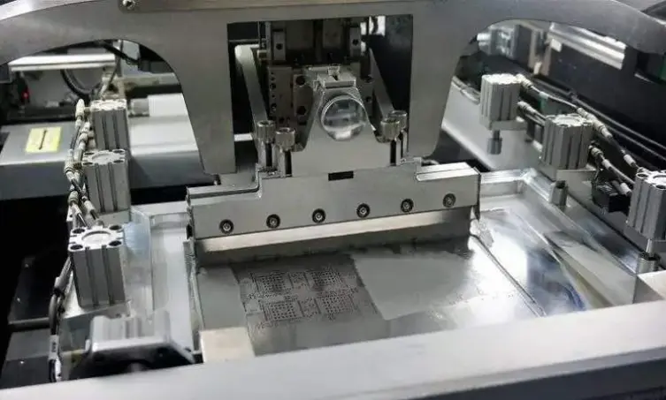
VIII. Solder Paste Printing Control
When changing the production line, refer to the settings in the production data folder and confirm the following printing quality:
- The SPI machine automatically detects (thickness, area, volume, short - circuit, missing printing, offset) and records each board.
- If the SPI cannot peRForm the detection due to the absence of an SPI machine or other abnormal reasons, conduct random inspections by personnel. Visually inspect the solder paste printing (no short - circuit, no missing printing, no offset or offset < 1/3 PAD), and submit a special procurement form for the process. The form will take effect and be archived after being signed by the relevant department supervisor.
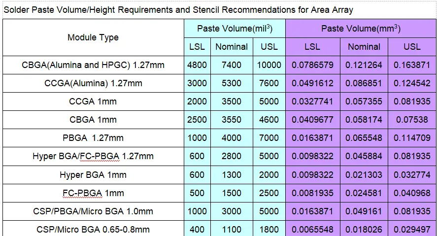
- Solder Paste Thickness & Volume Control:
- Solder Paste Thickness Control Reference Range: (The SPI machine mainly controls by volume, and the thickness is for auxiliary reference.)
- a. For 0.5 mm Pitch CSP / Micro BGA: T - 0.005mm ~ T + 0.055mm
- b. For 0.5 mm Pitch QFP / QFN: T - 0.005mm ~ T + 0.055mm
- c. For 0.8 - 1.0 mm Pitch BGA/ CSP: T - 0.005mm ~ T + 0.065mm
- d. For Normal Chip (RLC and others): T - 0.005mm ~ T + 0.085mm (Remark: T = stencil thickness)
- Solder Paste Volume Control (for SPI machine measurement):
- a. For 0.5 mm Pitch CSP / Micro BGA: 0.0016387 ~ 0.008194mm³
- b. For CSP/Micro BGA 0.65 - 0.8mm: 0.0065548 ~ 0.029497mm³
- c. For CSP/PBGA/Micro BGA 1.0mm: 0.0163871 ~ 0.081935mm³
- d. Refer to the following attachment for the volume control of other components.
- Solder Paste Thickness Control Reference Range: (The SPI machine mainly controls by volume, and the thickness is for auxiliary reference.)
-
- When using the SPI to inspect the solder paste printing quality, the operator should observe and record the CPK value and average thickness every 2 hours.