 PCB
PCB FPC
FPC Rigid-Flex
 FR-4
FR-4 HDI PCB
 Rogers High-Frequency Board
 PTFE Teflon High-Frequency Board
 Aluminum
 Copper Core
 PCB Assembly
 LED light PCBA
 Memory PCBA
 Power Supply PCBA
 New Energey PCBA
 Communication PCBA
 Industrial Control PCBA
 Medical Equipment PCBA
 Testing Service
 PCBA Testing Service
 Certification Application
 RoHS Certification Application
 REACH Certification Application
 CE Certification Application
 FCC Certification Application
 CQC Certification Application
 UL Certification Application
 Transformers, Inductors
 High Frequency Transformers
 Low Frequency Transformers
 High Power Transformers
 Conversion Transformers
 Sealed Transformers
 Ring Transformers
 Inductors
 Wires,Cables Customized
 Network Cables
 Power Cords
 Antenna Cables
 Coaxial Cables
 Net Position Indicator
 Solar AIS net position indicator
 Capacitors
 Connectors
 Diodes
 Embedded Processors & Controllers
 Digital Signal Processors (DSP/DSC)
 Microcontrollers (MCU/MPU/SOC)
 Programmable Logic Device(CPLD/FPGA)
 Communication Modules/IoT
 Resistors
 Through Hole Resistors
 Resistor Networks, Arrays
 Potentiometers,Variable Resistors
 Aluminum Case,Porcelain Tube Resistance
 Current Sense Resistors,Shunt Resistors
 Switches
 Transistors
 Power Modules
 Isolated Power Modules
 AC-DC Power Modules
 DC-AC Module(Inverter)
 RF and Wireless
Key points of DC-DC conversion design
Key points of DC-DC conversion design
DC-DC converters can achieve effICient power conversion and supply at various voltage levels. However, as demand continues to rise, there is a need for higher power density, greater efficiency, and smaller size. The PCB design for DC-DC conversion becomes even more important. Here are some key points for the PCB design of DC-DC converters:
Line length
In high-frequency converters, the length of traces carrying high-speed switching signals is crucial for maintaining signal integrity and reducing EMI.
Longer traces can act as antennas and radiate electromagnetic energy, which may cause interference with other components or circuits. In addition, longer traces may cause delays, signal reflections, and parasitic effects, resulting in reduced converter efficiency and stability.
Therefore, the length of the trace should be as short as possible, especially for high-speed clock and data clock. Proper impedance matching techniques and controlled impedance traces can further optimize signal transmission and minimize signal attenuation.
Loop area
The loop area refers to the enclosed area formed by the signal traces on the PCB and their return paths. In high-power and high-frequency circuits such as DC-DC converters, minimizing the loop area is crucial for reducing radiated EMI.
A larger loop area will result in more magnetic flux coupling with the loop, leading to higher EMI.
The main measure to minimize the loop area is to place the signal trace near its return path, such as using a ground plane/tightly spaced power plane, to minimize the loop area.
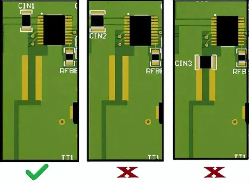
Device selection and capacitor placement
Adding ferrite beads and common mode chokes and other filter components in critical signal and power lines can attenuate conducted electromagnetic interference and prevent further propagation. When connecting the filter capacitor, the correct position is crucial for filtering out EMI.
Filter components should be placed as close as possible to the DC-DC converter. Properly placing decoupling capacitors near the power pins of ICs and active components can help suppress high-frequency noise and improve EMI performance.
Placement of decoupling capacitors
Parasitic inductance
Parasitic inductance is the inherent inductance of a conductive path, such as a trace/wire, depending on its physical size and material properties. In high-frequency circuits such as DC-DC converters, path inductance can affect the efficiency and performance of the converter.
High parasitic inductance can lead to voltage drop, increased switching losses, and reduced converter efficiency, and may also cause voltage overshoot and ringing in the circuit, affecting signal integrity.
To minimize parasitic inductance, PCB engineers can use wider traces, shorter paths, or create low-inductance return paths for high-current/switching signals using dedicated ground/power planes.
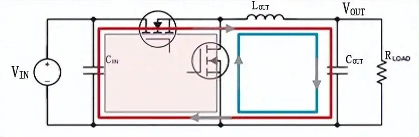
The impact of the grounding loop of the DC-DC converter
When designing a DC-DC converter, PCB engineers must consider the current loop and place components correctly so that the loop can be physically as small as possible.
Current loop in DC-DC converter
The following problems may be caused by too long grounding ring circuit:
Electromagnetic interference: The grounding loop can act as an antenna, causing EMI radiation into the surrounding environment.
Noise and signal attenuation: The current flowing through the grounding loop will generate voltage differences between different grounding points, which may cause unwanted noise to be introduced into sensitive signal paths, resulting in signal attenuation and reduced signal-to-noise ratio.
Common-mode noise: The ground loop may cause common-mode noise to couple into sensitive analog or digital circuits. This noise can destroy signal accuracy, especially in low-level analog measurements or high-speed digital communications.
· Parasitic grounding current: Circulating currents can flow between different grounding points, resulting in parasitic grounding currents. Parasitic currents can cause voltage drops and affect the performance of the converter, resulting in low efficiency and potential thermal issues.
Ground bounce: A grounded loop may cause a voltage difference between the ground reference planes, resulting in ground bounce. Ground bounce refers to the transient increase in ground voltage during switching, which can disrupt signal integrity and affect the normal operation of digital circuits.
Mitigation measures
Ground plane: Using a solid ground plane on the PCB ensures a low-impedance return path for current, thereby reducing the risk of ground loops.
Ground segmentation: Proper segmentation of the ground layers of different functional blocks or components can prevent ground currents from interfering with each other.
Separating analog and digital grounds: Physically separating analog and digital ground planes can prevent interference between sensitive analog circuits and noisy digital circuits.
Trace routing: Ensure that traces carrying high current or high frequency signals have low inductance return paths. For example, using short and wide traces or ground vias can help minimize the possibility of ground loops.