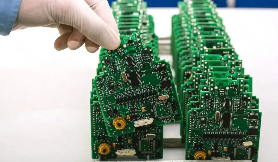
 PCB
PCB FPC
FPC Rigid-Flex
 FR-4
FR-4 HDI PCB
 Rogers High-Frequency Board
 PTFE Teflon High-Frequency Board
 Aluminum
 Copper Core
 PCB Assembly
 LED light PCBA
 Memory PCBA
 Power Supply PCBA
 New Energey PCBA
 Communication PCBA
 Industrial Control PCBA
 Medical Equipment PCBA
 Testing Service
 PCBA Testing Service
 Certification Application
 RoHS Certification Application
 REACH Certification Application
 CE Certification Application
 FCC Certification Application
 CQC Certification Application
 UL Certification Application
 Transformers, Inductors
 High Frequency Transformers
 Low Frequency Transformers
 High Power Transformers
 Conversion Transformers
 Sealed Transformers
 Ring Transformers
 Inductors
 Wires,Cables Customized
 Network Cables
 Power Cords
 Antenna Cables
 Coaxial Cables
 Net Position Indicator
 Solar AIS net position indicator
 Capacitors
 Connectors
 Diodes
 Embedded Processors & Controllers
 Digital Signal Processors (DSP/DSC)
 Microcontrollers (MCU/MPU/SOC)
 Programmable Logic Device(CPLD/FPGA)
 Communication Modules/IoT
 Resistors
 Through Hole Resistors
 Resistor Networks, Arrays
 Potentiometers,Variable Resistors
 Aluminum Case,Porcelain Tube Resistance
 Current Sense Resistors,Shunt Resistors
 Switches
 Transistors
 Power Modules
 Isolated Power Modules
 AC-DC Power Modules
 DC-AC Module(Inverter)
 RF and Wireless
Impact of Laser Cutting vs. Mechanical Milling on Component Mounting Accuracy in Subsequent PCB Assembly
2025-10-11
Context of PCB Contour Processing and Significance of Mounting Accuracy
PCB contour processing is the final step in shaping PCBs, defining the board’s external dimensions, notches, and cutouts to meet assembly fit requirements for end products (e.g., smartphone casings, automotive control Modules). Two mainstream technologies dominate this process: mechanICal milling (relying on rotating carbide cutters to remove material) and laser cutting (using high-energy laser beams to ablate substrate material).
Component mounting accuracy—measured by the deviation between the actual component position and its design coordinates—is critical for PCB assembly. For surface-mount technology (SMT) components (e.g., 0201 chips, BGA packages), even a 0.05mm positional deviation can cause solder joint defects (e.g., bridging, insufficient wetting) or electrical failures. Thus, understanding how contour processing methods affect mounting accuracy is essential for balancing PCB manufacturing efficiency, cost, and end-product reliability.
2. Core Differences in PCB Contour Quality Between Laser Cutting and Mechanical Milling
The impact of contour processing on mounting accuracy originates from differences in edge quality, dimensional precision, and substrate stress introduced by the two methods. These differences directly influence the PCB’s stability during SMT and the accuracy of component placement systems.
| Quality Metric | Laser Cutting | Mechanical Milling |
|---|---|---|
| Edge Roughness (Ra) | Ultra-low (≤0.3μm) – Laser ablation creates a smooth, burr-free edge without mechanical contact. | Higher (0.8–1.5μm) – Cutter wear or uneven feed rates cause burrs (height >0.1mm) and micro-chipping. |
| Dimensional Deviation | Minimal (±0.02mm) – Computer numerical control (CNC) laser positioning ensures high repeatability. | Larger (±0.05mm) – Cutter deflection (under 5–10N cutting force) and substrate deformation induce errors. |
| Substrate Internal Stress | Negligible – Non-contact processing avoids compressive/tensile stress in the substrate. | Significant – Mechanical force (15–25N) causes stress concentration, leading to post-processing warpage (0.1–0.3mm/m). |
| Edge Perpendicularity | Excellent (90°±0.1°) – Laser beam parallelism ensures vertical edges. | Poor (90°±0.5°) – Cutter runout or uneven substrate clamping leads to tapered edges. |
These differences form the foundation for how each method affects subsequent component mounting accuracy.
3. Impact on Component Mounting Accuracy: Laser Cutting vs. Mechanical Milling
Component mounting accuracy depends on two key factors: PCB flatness during SMT (affected by residual stress) and positional reference reliability (affected by edge precision and dimensional stability). Below is a detailed comparison of the two methods’ impacts:
3.1 Impact of Laser Cutting on Mounting Accuracy
Laser cutting’s non-contact, low-stress characteristics provide significant advantages for mounting accuracy, especially for high-density and miniaturized PCBs:
- Minimal Warpage Ensures Stable SMT Clamping: Laser cutting avoids mechanical force, so PCBs retain flatness (warpage ≤0.05mm/m) after processing. During SMT, the PCB lies flat on the mounting table, preventing "tilt-induced deviation" of the placement head (which can reach 0.03mm for warped boards). For example, 0.8mm-thick flexible PCBs processed by laser maintain flatness within ±0.02mm, ensuring 0201 components (pad size 0.25×0.12mm) are mounted with positional deviation <0.01mm.
- Precise Edges Enhance Reference Accuracy: SMT placement systems use PCB edges or fiducial marks as positional references. Laser-cut edges (dimensional deviation ±0.02mm) ensure the system’s vision camera accurately identifies the PCB’s coordinate system. For BGA packages (pitch 0.5mm), this reduces "reference offset" from 0.04mm (mechanical milling) to 0.01mm, lowering solder joint void rates by 15–20%.
- No Burrs Eliminate Interference with Small Components: Laser-cut edges have no burrs, avoiding physical obstruction of component placement. For micro-components like 01005 chips (length 0.4mm), burrs from mechanical milling (height >0.1mm) can push the component off-target by 0.03–0.05mm; laser cutting eliminates this risk, keeping placement deviation <0.02mm.
3.2 Impact of Mechanical Milling on Mounting Accuracy
Mechanical milling’s contact-based processing introduces challenges that degrade mounting accuracy, particularly for thin, flexible, or high-precision PCBs:
- Residual Stress Causes Post-Processing Warpage: The compressive force of the milling cutter (15–25N) induces internal stress in the PCB. After processing, stress relaxation leads to warpage (0.1–0.3mm/m for FR-4 PCBs), which is amplified during SMT preheating (80–120℃). For example, a 1.6mm-thick PCB with 0.2mm/m warpage may cause a QFP (quad flat package) to shift by 0.04mm, increasing the risk of pin bridging.
- Edge Burrs and Dimensional Errors Disrupt Reference Alignment: Milled edges often have burrs (height 0.1–0.2mm) and dimensional deviations (±0.05mm), which confuse the SMT vision system. When the system uses the edge as a reference, it may misalign the PCB coordinate system by 0.03–0.06mm. For fine-pitch components (e.g., 0.4mm pitch QFP), this misalignment can result in 10–15% of pins failing to align with pads.
- Cutter Runout Induces Tapered Edges: Cutter runout (0.01–0.03mm) during milling creates tapered edges (angle deviation 0.5–1°), which reduce the accuracy of mechanical clamping in SMT. The PCB may shift slightly during placement, causing positional deviation of 0.02–0.04mm for chip components (e.g., 0603 resistors).
4. Application-Specific Recommendations: Choosing the Right Contour Method
The choice between laser cutting and mechanical milling depends on component type, PCB density, and end-product requirements. The following guidelines help optimize mounting accuracy:
| Application Scenario | Recommended Method | Rationale for Mounting Accuracy |
|---|---|---|
| High-Density PCBs (≥100 components/in²) | Laser Cutting | Ultra-low edge roughness and minimal warpage ensure 01005/0201 components are mounted with <0.02mm deviation. |
| Fine-Pitch Components (pitch ≤0.5mm, e.g., BGA) | Laser Cutting | Precise dimensional control (±0.02mm) reduces reference offset, lowering solder joint void rates. |
| Thin/Flexible PCBs (thickness ≤0.8mm) | Laser Cutting | Non-contact processing avoids stress-induced warpage, critical for flexible PCB mounting stability. |
| Low-Cost, Low-Density PCBs (e.g., toy PCBs) | Mechanical Milling | For components with large pads (e.g., 0805 resistors), ±0.05mm deviation is acceptable, and milling reduces costs by 30–50%. |
| Thick PCBs (thickness ≥3mm, e.g., power boards) | Mechanical Milling | Thick substrates resist warpage; milling’s higher cutting efficiency suits large contour sizes. |
5. Mitigation Strategies for Mechanical Milling’s Accuracy Limitations
For scenarios where mechanical milling is preferred (e.g., cost constraints), the following measures can mitigate its impact on mounting accuracy:
- Cutter Maintenance: Replace carbide cutters every 500–800 meters of cutting to avoid wear-induced burrs. Use diamond-coated cutters for FR-4 substrates to reduce edge roughness to 0.5–0.8μm.
- Stress Relief: After milling, bake PCBs at 120–150℃ for 30–60 minutes to release residual stress, reducing warpage by 40–60% (from 0.3mm/m to 0.1–0.15mm/m).
- Post-Processing Deburring: Use plasma cleaning (power 300–400W, time 60 seconds) or abrasive brushing to remove burrs, ensuring edge roughness ≤0.6μm.
- Fiducial Mark Optimization: Add 2–3 extra fiducial marks (diameter 1mm, tolerance ±0.01mm) on the PCB to allow the SMT system to correct for dimensional deviations, reducing reference offset by 50%.