 PCB
PCB FPC
FPC Rigid-Flex
 FR-4
FR-4 HDI PCB
 Rogers High-Frequency Board
 PTFE Teflon High-Frequency Board
 Aluminum
 Copper Core
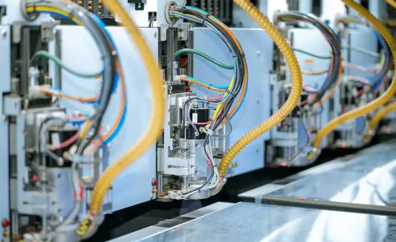
 PCB Assembly
 LED light PCBA
 Memory PCBA
 Power Supply PCBA
 New Energey PCBA
 Communication PCBA
 Industrial Control PCBA
 Medical Equipment PCBA
 Testing Service
 PCBA Testing Service
 Certification Application
 RoHS Certification Application
 REACH Certification Application
 CE Certification Application
 FCC Certification Application
 CQC Certification Application
 UL Certification Application
 Transformers, Inductors
 High Frequency Transformers
 Low Frequency Transformers
 High Power Transformers
 Conversion Transformers
 Sealed Transformers
 Ring Transformers
 Inductors
 Wires,Cables Customized
 Network Cables
 Power Cords
 Antenna Cables
 Coaxial Cables
 Net Position Indicator
 Solar AIS net position indicator
 Capacitors
 Connectors
 Diodes
 Embedded Processors & Controllers
 Digital Signal Processors (DSP/DSC)
 Microcontrollers (MCU/MPU/SOC)
 Programmable Logic Device(CPLD/FPGA)
 Communication Modules/IoT
 Resistors
 Through Hole Resistors
 Resistor Networks, Arrays
 Potentiometers,Variable Resistors
 Aluminum Case,Porcelain Tube Resistance
 Current Sense Resistors,Shunt Resistors
 Switches
 Transistors
 Power Modules
 Isolated Power Modules
 AC-DC Power Modules
 DC-AC Module(Inverter)
 RF and Wireless
How is the circuit board produced? Detailed explanation of the production process of PCB circuit boards.
How is the Circuit Board produced? Detailed explanation of the production process of PCB circuit boards.
PCB Printed Circuit Board is the core component of electronIC products, providing physical support and electrical connection for electronic components. With the increasing complexity of electronic devices, PCB production processes have gradually evolved into more complex and refined processes, especially for the manufacture of high-layer PCBs, which place higher demands on materials, precision, and processes.
For electronic engineers, understanding the PCB production process can not only further optimize the layout design, but also improve product quality and accelerate the R&D progress.
Production process of PCB circuit board
According to the number of copper foil layers, PCB can be divided into single-sided, double-sided and multi-layer boards; From the perspective of type, PCB can be divided into hard board, soft board, soft and hard board, etc. Here we mainly introduce the production process of FR-4 substrate rigid PCB.
Cutting and drilling
The first step in production is to cut the copper clad laminate to the required size according to design requirements. The cutting process requires precise cutting to ensure that the material size meets the requirements of subsequent processing, avoiding waste or problems in subsequent processes caused by dimensional deviations. Typically, automated panel cutting equipment is used to maintain high efficiency and precision.
Then, use a high-precision drilling machine to drill precise through-holes on the circuit board. These holes will be used for electrical connections between different layers, although in a single-layer PCB, the holes are mainly used to mount through-hole components. During the drilling process, it is necessary to use appropriate drill diameters and precise drilling parameters to ensure smooth and burr-free hole walls, avoiding affecting the subsequent copper deposition process.
Sinking copper
After drilling, the hole wall of the PCB needs to be bulking and chemically treated to ensure good adhesion. Firstly, the bulking treatment of the hole wall helps to increase the roughness of the hole wall, thereby enhancing the adhesion of copper. Subsequently, through electrochemical methods, copper ions in the electrolyte are uniformly deposited on the pore walls, forming a thin and uniform copper foil layer. This layer of copper is crucial for ensuring the conductivity of the hole and is the basis for achieving electrical connection.
Line exposure
In this process, PCB manufacturers use LDI laser direct imaging technology to accurately project the circuit diagram in the CAM data onto the copper cladding layer of the PCB. At this time, the surface of the plate is pre-coated with a photosensitive dry film. After being exposed to strong ultraviolet light, the dry film undergoes a polymerization reaction, and some areas are initially cured. This process determines the final shape of the circuit and is a very critical step in the PCB manufacturing process.
After exposure, the development process will remove the unexposed dry film, leaving the cured dry film to protect the copper foil area that needs to be preserved. The developed board will show the embryonic form of the circuit diagram.
electroplate
Electroplating is an important step in PCB manufacturing, the main purpose of which is to further increase the thickness of the copper layer on the developed lines and hole walls to ensure its electrical conductivity and mechanical strength. First, the PCB is installed on the electroplating production line, and after surface pretreatment such as degreasing and pickling, the copper surface is ensured to be clean and free of contamination.
Then, a uniform thickness of copper is plated on the exposed lines and hole walls through electrochemical reaction, followed by a layer of tin plating on the surface of the copper layer. The role of this layer of tin is to protect the circuit from being removed during the subsequent etching process.
Resin/copper paste plug hole
During the PCB manufacturing process, after drilling and metallizing the holes to be plugged using a special process, the aluminum sheet that was previously laser-drilled is made into an aluminum sheet stencil and installed on a vacuum plugging machine. Next, the resin/copper paste is inserted into the corresponding hole, and after high-temperature curing and resin grinding, the hole is smoothed. Finally, an electroplated cap is formed through electroplating technology, restoring the drilled pad into a whole. This process is also known as the disk hole process. It can not only greatly improve the efficiency of PCB design engineers, but also solve the problem of wiring space and improve the yield of PCB.
surface treatment
In order to protect the circuit board and improve its soldering performance, surface treatment is one of the last key steps. Common surface treatment methods include HASL (Hot Air Solder Leveling), HASL, ENIG (Electroless Nickel Immersion Gold), and ENIG.
Soldering: The board is immersed in molten tin, and then the excess tin is blown off with a hot air knife to form a uniform pad surface. This method is less expensive, but the flatness is not as good as immersion gold.
Immersion gold: A layer of nickel is plated on the surface of copper, followed by a layer of gold to prevent oxidation of copper and provide excellent soldering performance. The pad treated with immersion gold has high flatness, suitable for soldering components with fine pitch, and is a common choice for high-layer and high-precision PCBs.
Inspection and Testing
After production, the circuit board needs to undergo a series of quality tests, including AOI automatic optical inspection, X-ray inspection, and functional testing, to ensure that each board can work properly.
The production process of PCB circuit boards is a key link to ensure product performance and quality. Minintel ensures that each PCB can bring reliable performance and stable quality to customers through leading equipment, precise processes, and strict quality control. Whether it is complex high-level multi-layer design or high-frequency applications, Minintel can provide strong support for electronic engineers to help them turn their ideas into efficient products.