 PCB
PCB FPC
FPC Rigid-Flex
 FR-4
FR-4 HDI PCB
 Rogers High-Frequency Board
 PTFE Teflon High-Frequency Board
 Aluminum
 Copper Core
 PCB Assembly
 LED light PCBA
 Memory PCBA
 Power Supply PCBA
 New Energey PCBA
 Communication PCBA
 Industrial Control PCBA
 Medical Equipment PCBA
 Testing Service
 PCBA Testing Service
 Certification Application
 RoHS Certification Application
 REACH Certification Application
 CE Certification Application
 FCC Certification Application
 CQC Certification Application
 UL Certification Application
 Transformers, Inductors
 High Frequency Transformers
 Low Frequency Transformers
 High Power Transformers
 Conversion Transformers
 Sealed Transformers
 Ring Transformers
 Inductors
 Wires,Cables Customized
 Network Cables
 Power Cords
 Antenna Cables
 Coaxial Cables
 Net Position Indicator
 Solar AIS net position indicator
 Capacitors
 Connectors
 Diodes
 Embedded Processors & Controllers
 Digital Signal Processors (DSP/DSC)
 Microcontrollers (MCU/MPU/SOC)
 Programmable Logic Device(CPLD/FPGA)
 Communication Modules/IoT
 Resistors
 Through Hole Resistors
 Resistor Networks, Arrays
 Potentiometers,Variable Resistors
 Aluminum Case,Porcelain Tube Resistance
 Current Sense Resistors,Shunt Resistors
 Switches
 Transistors
 Power Modules
 Isolated Power Modules
 AC-DC Power Modules
 DC-AC Module(Inverter)
 RF and Wireless
Part I: Formation and Application of the Theory of Wave Soldering Dynamics
Part I: Formation and ApplICation of the Theory of Wave Soldering Dynamics
I. Overview
1. Formation of the Theory of Solder Wave Dynamics
Theoretically, wave soldering is a logical extension of dip soldering. The fundamental difference between dip soldering and wave soldering lies in the method of immersion: dip soldering uses a static liquid suRFace of molten solder for immersion, while wave soldering employs a wave of molten solder for immersion. The solder wave generator constitutes the core of the wave soldering equipment system and is also a key technology in the design of wave soldering equipment systems. It is well-known that the performance of the solder wave generator determines the overall functionality of the system.
The solder wave generator is the dynamic system that generates the wave of liquid metal solder. The generation of the liquid metal solder wave, its stability, the design of the working wave shape, the thermal characteristics of the solder wave, the ability to inhibit the oxidation of high-temperature molten solder, the wettability of the substrate metal to be welded, and the influence on the conformal coating of solder joints all exhibit certain regularities. Describing these regularities involves knowledge of fluid mechanics, electromagnetic fluid mechanics (for electromagnetic pumps), metallurgy, surface theory of metals, thermal engineering, and other related fields. Often, solving a problem requires the intersection and penetration of knowledge from these disciplines. Thus, they collectively constitute the basic content of the theory of solder wave dynamics.
2. Guiding Significance of the Theory of Solder Wave Dynamics for the Development of Wave Soldering Technology
The research findings of the theory of solder wave dynamics not only enable the achievement of high-quality solder joints that are smooth, glossy, conformal, and free of defects such as drawing and burrs, but also reveal a series of constraints and fundamental principles that should be followed in the design of solder wave generators.
* Due to the high temperatures, the immersion time of the PCB in the solder should not be too long. However, from a metallurgical perspective, in order to obtain good solder joints, it is necessary to maintain sufficient contact time between the PCB and the solder to allow the welding area to receive enough heat to reach a good wetting temperature.
* When the molten liquid solder flows under the PCB, it causes a scrubbing effect on the welding area, which aids in melting. Therefore, the solder wave should have a longer contact time with the PCB while minimizing the generation of solder dross, i.e., minimizing the contact between the wave and the air.
* To reduce drawing and bridging, the movement speed of the PCB relative to the solder should be close to zero when the PCB exits the wave.
* When the PCB passes through the wave, the solder wave should be flat and smooth, allowing full contact with the entire welding surface of the PCB. An uneven wave can cause molten solder to overflow onto the component side of the PCB or result in partial missing solder.
* The generation of solder dross must be minimized as it can accelerate wear on the solder pump system (for mechanical pumps) and cause uneven waves. Excessive solder dross can also accelerate the consumption of major components such as tin in the solder, which not only increases production costs but also seriously pollutes the environment.
To obtain the best results in wave soldering, it is necessary to properly address the above issues and satisfy these conflicting conditions as much as possible.
These contents constitute the research focus of the theory of solder wave dynamics. It is also the research findings and applications of the theory of solder wave dynamics that have made wave soldering one of the main welding methods for PCBs, especially in large-scale production.
II. Dynamic Phenomena of the Solder Wave in Wave Soldering
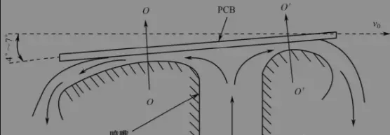
For the sake of discussion, let's approximate the liquid solder flow clamped between the PCB and the wave nozzle wall during wave soldering as SIMilar to the flow of a viscous fluid in a rectangular pipe, as shown in the diagram below.
Fluid mechanics theory tells us that when a fluid flows in a pipe, the fluid's own cohesion (viscosity) and the adhesion between the fluid and the solid wall create velocity differences throughout the fluid. The fluid close to the pipe wall will adhere to it, with a relative velocity of zero, meaning there is no slip of the fluid on the wall surface. Near the wall, as the normal distance from the wall increases, the wall's influence on the fluid weakens, and the fluid's velocity will rapidly increase until it reaches a velocity close to the original, undisturbed velocity at a certain distance. Therefore, the velocity change occurs only within a thin layer adjacent to the wall, known as the boundary layer or attached layer.
For convenience in analysis, we first intercept two cross-sections perpendicular to the solder flow velocity on both sides of the nozzle, namely the O-O cross-section (as shown in Figure 1 below) and the O'-O' cross-section (as shown in Figure 2 below), to analyze their velocity distribution patterns. Set N-N and M-M as the centerlines of the O-O and O'-O' cross-sections, respectively, and discuss the following two cases.
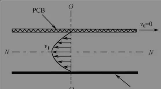
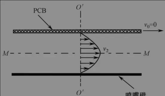
(1) When the PCB is stationary, i.e., v0=0, as mentioned earlier, due to the fluid wall attachment effect and cohesion, the velocity distribution of the solder fluid clamped between the PCB and the nozzle wall is parabolic, with the velocity close to the PCB surface and the nozzle wall being zero, and the maximum velocity occurring at the centerline.
(2) When the PCB is moving, and v0 = vx, when the PCB moves in the direction indicated by the countercurrent arrow with v0=vx, the distribution of fluid velocity in the O-O and O'-O' cross-sections changes, as shown in the following two diagrams:
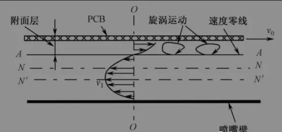
Velocity distribution in the pipe when the PCB moves in the opposite direction;
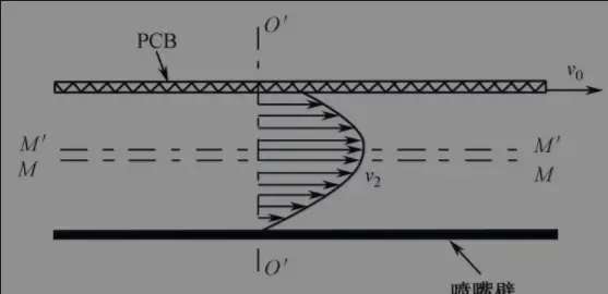
Velocity distribution in the pipe when the PCB moves in the same direction.
According to fluid mechanics laws, the tangential velocity v0 of a viscous fluid particle in the tangential direction of the wall is equal to the tangential velocity vC of the corresponding point on the rigid wall, i.e., vC = v0. In other words, the fluid particles close to the boundary wall and the corresponding points on the wall have the same velocity. Obviously, in the case of the O-O cross-section as shown in Figure 2.4, the fluid velocity zero point will no longer appear on the boundary wall but will shift to the A-A surface inside the fluid, and the maximum velocity line in the pipe will also shift from N-N to the N'-N' surface. We call the fluid layer between the velocity zero line and the lower side of the PCB the attached layer. At this point, all vortex motion of the incoming flow is concentrated within the attached layer, and the tangential velocity along the PCB surface varies greatly within this layer, resulting in a large velocity gradient in the normal direction of the PCB surface. In other words, there is considerable vortex motion in the fluid, which will intensify the adhesion of viscous fluid particles to the rigid wall. According to this theory, when the PCB and the liquid solder move relatively during wave soldering, it is inevitable that a considerable amount of liquid solder adhered to the surface of the substrate metal to be welded will be carried forward together. This constitutes the necessary conditions for icicle formation and bridging. Moreover, the faster the PCB moves (v0) relative to the countercurrent velocity of the fluid in the wave (v1), the more solder is carried, and the more severe the icicle formation and bridging. Therefore, slowing down the PCB's movement speed (v0) or speeding up the countercurrent fluid velocity (v1) can compress the thickness of the attached layer, thereby effectively suppressing the vortex motion within it. The amount of excess solder adhering to the PCB wall and moving with it is greatly reduced, effectively inhibiting the probability of icicle formation and bridging, which has been proven by extensive production practice.
However, the situation for the O'-O' cross-section shown in Figure 2.5 differs from the O-O cross-section shown in Figure 2.4. Since the PCB's movement direction (v0) is the same as the fluid's forward flow velocity direction (v2) at this time, there is no issue of an attached layer, and therefore no vortex motion formed by solder recirculation. Adjusting the size of the fluid's forward flow velocity (v2) can achieve optimal detachment conditions at the point where the PCB separates from the wave.