 PCB
PCB FPC
FPC Rigid-Flex
 FR-4
FR-4 HDI PCB
 Rogers High-Frequency Board
 PTFE Teflon High-Frequency Board
 Aluminum
 Copper Core
 PCB Assembly
 LED light PCBA
 Memory PCBA
 Power Supply PCBA
 New Energey PCBA
 Communication PCBA
 Industrial Control PCBA
 Medical Equipment PCBA
 Testing Service
 PCBA Testing Service
 Certification Application
 RoHS Certification Application
 REACH Certification Application
 CE Certification Application
 FCC Certification Application
 CQC Certification Application
 UL Certification Application
 Transformers, Inductors
 High Frequency Transformers
 Low Frequency Transformers
 High Power Transformers
 Conversion Transformers
 Sealed Transformers
 Ring Transformers
 Inductors
 Wires,Cables Customized
 Network Cables
 Power Cords
 Antenna Cables
 Coaxial Cables
 Net Position Indicator
 Solar AIS net position indicator
 Capacitors
 Connectors
 Diodes
 Embedded Processors & Controllers
 Digital Signal Processors (DSP/DSC)
 Microcontrollers (MCU/MPU/SOC)
 Programmable Logic Device(CPLD/FPGA)
 Communication Modules/IoT
 Resistors
 Through Hole Resistors
 Resistor Networks, Arrays
 Potentiometers,Variable Resistors
 Aluminum Case,Porcelain Tube Resistance
 Current Sense Resistors,Shunt Resistors
 Switches
 Transistors
 Power Modules
 Isolated Power Modules
 AC-DC Power Modules
 DC-AC Module(Inverter)
 RF and Wireless
Localizing Open Circuits Detected by Flying Probe/ICT but Undetected by AOI and Visual Inspection
2026-01-13

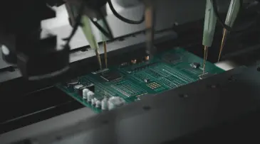
In modern printed circuit board (PCB) assembly manufacturing, a multi-layered quality control (QC) system—integrating Automated Optical Inspection (AOI), manual visual inspection, and electrical testing (such as Flying Probe Testing and In-Circuit Testing, ICT)—is widely adopted to ensure product reliability. Among these, electrical testing (Flying Probe/ICT) is regarded as the final "gatekeeper" for identifying electrical connectivity defects, as it directly verifies the functional integrity of the PCB assembly. A common and perplexing scenario in production is the detection of open circuits by Flying Probe or ICT, while AOI and visual inspection fail to identify any corresponding physical defects. This diSCRepancy poses significant challenges to manufacturing engineers, as it implies the open circuit is either hidden, microscopic, or related to non-visible factors such as material properties or internal structural failures.
Open circuits in this context refer to interruptions in the intended electrical path between two or more nodes on the PCBassembly, resulting in the loss of electrical continuity. Unlike visible defects such as solder bridges, missing components, or obvious solder joint voids— which are easily captured by AOI and visual inspection—open circuits undetected by optical methods often stem from subtle issues: incomplete solder joint formation beneath component bodies, micro-cracks in copper traces, delamination between PCB layers, poor wetting between solder and pads without visible anomalies, or even transient connectivity issues caused by thermal or mechanical stress. The failure of AOI and visual inspection to detect these issues is not a flaw in these technologies but a reflection of their inherent limitations—they rely on optical contrast and geometric analysis, which are ineffective for defects that do not alter the suRFace appearance or geometry of the assembly.
The ability to accurately localize such open circuits is critical for minimizing production downtime, reducing rework costs, and ensuring the reliability of the final product. Incorrect or delayed localization can lead to unnecessary scrapping of PCBs, extended production cycles, and even the shipment of defective products, which may result in field failures and damage to brand reputation. This article provides a comprehensive guide to addressing this challenge, first analyzing the fundamental reasons for the discrepancy between electrical testing results and optical inspection findings. It then details a systematic, layered localization methodology, covering advanced non-destructive testing (NDT) techniques, destructive verification methods, and data-driven analysis approaches. Additionally, it includes case studies to illustrate the application of these methods in real-world scenarios and summarizes preventive measures to reduce the occurrence of such elusive open circuits.
1. Understanding the Discrepancy: Why Open Circuits Evade Optical Inspection
To effectively localize open circuits detected by Flying Probe/ICT but not by AOI/visual inspection, it is first essential to understand why these defects evade optical detection. This requires a clear comprehension of the working principles of each testing technology and the characteristics of the open circuits that cause the discrepancy.
AOI systems operate by capturing high-resolution images of the PCB assembly and comparing them to a pre-defined "golden standard" (a digital model of a defect-free assembly). They detect defects by identifying deviations in color, shape, size, or position of components, solder joints, or traces. AOI is highly effective for surface defects such as missing solder, excess solder, solder bridges, component misalignment, or damaged component bodies. However, it cannot "see" beneath component packages, inside solder joints, or through PCB layers. For example, a solder joint beneath a quad flat package (QFP) or a ball grid array (BGA) that has poor wetting (resulting in an open circuit) will not be visible to AOI. Similarly, micro-cracks in copper traces that are on the inner layers of a multi-layer PCB or are too small to alter the surface appearance will escape AOI detection.
Manual visual inspection, while more flexible than AOI, suffers from similar limitations. Even with the aid of magnifying glasses or stereo microscopes, human inspectors cannot observe defects hidden beneath components, inside through-holes, or in inner PCB layers. Additionally, visual inspection is subjective and prone to human error, especially when detecting extremely subtle surface defects (e.g., micro-voids in solder joints that do not affect the external shape of the joint). In many cases, open circuits caused by issues such as incomplete solder wetting or trace micro-cracks do not produce any visible surface anomalies, making them undetectable by visual inspection.
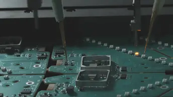
In contrast, Flying Probe Testing and ICT directly measure the electrical continuity of the PCB assembly. Flying Probe Testing uses movable probes to make contact with test points on the PCB, applying a small voltage and measuring current to verify connectivity between nodes. It is flexible and suitable for low-volume production or prototype testing. ICT, on the other hand, uses a custom test fixture with fixed probes that contact multiple test points simultaneously, enabling high-speed testing for high-volume production. Both technologies can detect open circuits by identifying a lack of current flow between two nodes that should be electrically connected, regardless of whether the defect has a visible manifestation. This is why they can detect open circuits that AOI and visual inspection miss—they measure electrical functionality, not just physical appearance.

1.1 Limitations of AOI and Visual Inspection
The open circuits that cause this discrepancy can be categorized into several types based on their root causes: solder joint-related defects, trace-related defects, component-related defects, and PCB structural defects. Solder joint-related defects are the most common, including incomplete wetting, cold solder joints, solder voids, and solder joint cracks. Incomplete wetting occurs when molten solder fails to fully adhere to the pad or component lead, resulting in a weak or non-existent electrical connection. Cold solder joints, caused by insufficient heating during soldering, have a granular, dull appearance, but in some cases, they may appear normal visually while lacking electrical continuity. Solder voids—small cavities within the solder joint—can reduce the cross-sectional area of the electrical path; if the voids are large enough or concentrated in a critical area, they can cause an open circuit. Solder joint cracks, which may be microscopically small or located beneath the component, can also lead to open circuits without visible surface signs.
Trace-related defects include micro-cracks in copper traces, trace delamination, and trace corrosion. Micro-cracks in traces can be caused by thermal stress during soldering or rework, mechanical stress during handling or assembly, or poor PCB manufacturing quality. These cracks are often too small to be detected by visual inspection or AOI but can interrupt electrical continuity. Trace delamination—where the copper trace separates from the PCB substrate—occurs due to excessive thermal stress or poor adhesion between the trace and substrate. This defect is typically hidden beneath the solder mask or component packages, making it undetectable by optical methods. Trace corrosion, caused by exposure to moisture, chemicals, or contaminants, can thin the trace to the point of open circuit, and early-stage corrosion may not be visible.
Component-related defects include internal open circuits in components, poor component lead coplanarity, and insufficient solderability of component leads. Internal open circuits—such as a broken bond wire inside an integrated circuit (IC)—cannot be detected by AOI or visual inspection, as the component exterior appears normal. Poor lead coplanarity (where some leads are not flush with the PCB surface) can result in incomplete solder joint formation, leading to open circuits that may not be visible if the component body obscures the affected leads. Insufficient solderability of leads (caused by oxidation or contamination) can lead to poor wetting and open circuits, even if the leads appear visually clean.
PCB structural defects such as via cracks, layer delamination, and substrate damage can also cause open circuits. Vias—conductive holes that connect different layers of a multi-layer PCB—can develop cracks due to thermal cycling or mechanical stress, interrupting the electrical path between layers. Layer delamination can separate internal traces, leading to open circuits that are completely hidden from view. Substrate damage, such as cracks or breaks in the PCB substrate, can also damage traces or vias, causing open circuits that may not be visible on the surface.
2. Systematic, Layered Localization Methodology
Localizing open circuits that evade AOI and visual inspection requires a systematic, layered approach that builds on the information provided by Flying Probe/ICT testing. The process should start with data analysis to narrow down the potential defect location, followed by non-destructive testing (NDT) techniques to further refine the location, and finally, if necessary, destructive testing to confirm the defect. This layered approach minimizes the risk of damaging the PCB assembly unnecessarily and ensures that the localization process is efficient and accurate.
The first step in the localization process is to analyze the data from the Flying Probe/ICT test. This data is critical for narrowing down the potential defect area. Engineers should first verify the test program to ensure that the open circuit detection is not a false positive caused by a programming error (e.g., incorrect test point assignments, wrong node connectivity definitions, or probe contact issues). False positives can occur if the test probes fail to make proper contact with the test points (due to contamination, oxide layers, or probe wear), leading the system to incorrectly detect an open circuit. To rule out false positives, engineers can re-run the test with cleaned test points, replace worn probes, or verify the test program against the PCB design files (Gerber files, BOM, netlist).
Once false positives are ruled out, engineers should analyze the specific net (electrical path) where the open circuit is detected. The netlist (a list of all electrical connections on the PCB) can be used to identify all components, traces, vias, and test points associated with the faulty net. This helps to narrow down the potential defect location to the nodes and interconnects within that net. For example, if the open circuit is detected between test point TP1 and component pin U1-5, the defect must be located along the path connecting TP1 to U1-5, which may include traces, vias, and solder joints at TP1 and U1-5.
Additional data from the test, such as the resistance value measured between the two nodes (if available), can provide further insights. A very high resistance (approaching infinity) typically indicates a complete open circuit, while a high but non-infinite resistance may indicate a partial open circuit (e.g., a micro-crack with some residual connectivity or a solder joint with poor wetting). The test data may also indicate whether the open circuit is consistent (detected every time the test is run) or intermittent. Intermittent open circuits are often caused by defects that are sensitive to temperature, humidity, or mechanical stress (e.g., micro-cracks that open and close with thermal expansion or contraction), which require specialized localization methods.
2.1 Step 1: Data Analysis from Flying Probe/ICT Testing
After narrowing down the potential defect area through data analysis, the next step is to use non-destructive testing (NDT) techniques to further refine the location. NDT techniques are preferred because they do not damage the PCB assembly, allowing for rework or further testing if needed. The choice of NDT technique depends on the type of potential defect and the accessibility of the area.
High-Magnification Optical Inspection (HMOI) is a more detailed form of visual inspection that uses high-power microscopes (50-200x magnification) to examine the potential defect area. While standard visual inspection may miss subtle defects, HMOI can reveal micro-cracks in traces, small voids in solder joints, or poor wetting that is not visible to the naked eye. For example, a solder joint with incomplete wetting may appear normal at low magnification but can be identified at high magnification by the presence of a non-uniform solder fillet, a high wetting angle, or exposed pad areas. HMOI is particularly effective for examining solder joints on the edges of component packages or test points that are accessible.
X-Ray Inspection is one of the most powerful NDT techniques for localizing hidden open circuits. X-ray systems use penetrating radiation to create images of the internal structure of the PCB assembly, allowing engineers to visualize defects beneath component packages, inside through-holes, and in multi-layer PCBs. X-ray inspection is especially effective for detecting defects in BGA, QFP, and other fine-pitch components, where solder joints are hidden beneath the component body. It can reveal solder joint voids, incomplete solder filling, cold solder joints, and via cracks that are completely invisible to optical inspection. For example, an open circuit caused by a void-filled solder joint beneath a BGA can be clearly visualized using X-ray inspection, as the voids appear as dark areas in the solder joint. 3D X-ray inspection (computed tomography, CT) provides even more detailed information by creating a 3D model of the assembly, allowing engineers to examine the defect from multiple angles and measure the size and location of voids or cracks with high precision.
Thermal Imaging (Thermography) is a useful technique for localizing intermittent open circuits or defects that are sensitive to temperature. Thermal imaging cameras detect the heat emitted by the PCB assembly when an electrical current is applied. In a normal circuit, current flows uniformly, producing a consistent heat pattern. An open circuit will interrupt current flow, resulting in a cold spot (an area with lower temperature than the surrounding area). For intermittent open circuits, engineers can apply thermal stress (heating or cooling the assembly) while monitoring the thermal image to identify the location where the cold spot appears when the open circuit occurs. Thermal imaging is also effective for detecting trace micro-cracks that open under thermal stress, as the crack will create a cold spot in the thermal image.
Ultrasonic Inspection uses high-frequency sound waves to detect defects in the PCB assembly. When sound waves pass through the assembly, they are reflected differently by different materials (e.g., solder, copper, substrate) and by defects (e.g., delamination, cracks, voids). Ultrasonic inspection is particularly effective for detecting PCB layer delamination, trace delamination, and internal component defects. It can also be used to examine the integrity of solder joints beneath components. For example, delamination between a copper trace and the PCB substrate will cause a distinct reflection of the ultrasonic waves, allowing engineers to locate the delaminated area. Ultrasonic inspection is non-invasive and can be used on both assembled and unassembled PCBs.
Electrical Continuity Testing with Precision Probes is a targeted electrical testing method that builds on the initial Flying Probe/ICT results. Using a precision probe station (equipped with micro-probes that can access small areas), engineers can test the continuity of specific segments of the faulty net. By systematically testing different points along the net (e.g., between a test point and a via, between a via and a component pin), engineers can narrow down the open circuit to a specific segment. For example, if continuity is present between TP1 and via V1 but not between V1 and U1-5, the open circuit must be located between V1 and U1-5 (e.g., in the trace from V1 to U1-5, the solder joint at U1-5, or via V1 itself). This method is highly accurate but requires access to the test points and nodes along the net, which may be challenging if they are hidden beneath components.
2.2 Step 2: Non-Destructive Testing (NDT) Techniques
If non-destructive testing techniques are unable to definitively locate the open circuit, destructive testing methods may be necessary. Destructive testing involves physically modifying the PCB assembly to expose the potential defect, which means the assembly may be damaged beyond repair. Therefore, these methods should only be used as a last resort, and preferably on scrap or redundant assemblies that are identical to the faulty one.
Decapsulation is a destructive technique used to examine the internal structure of components. If the open circuit is suspected to be caused by an internal component defect (e.g., a broken bond wire in an IC), decapsulation involves removing the component's plastic or ceramic package to expose the internal die and bond wires. This can be done using chemical etching (for plastic packages) or mechanical grinding (for ceramic packages). Once the package is removed, engineers can use a high-power microscope to examine the bond wires, die pads, and internal connections for defects. Decapsulation is a specialized technique that requires careful handling to avoid damaging the internal components.
Solder Joint Removal (Desoldering) involves removing components from the PCB to examine the underlying solder joints and pads. If the open circuit is suspected to be in a solder joint beneath a component (e.g., QFP, BGA), desoldering the component allows engineers to inspect the solder joints and pads directly. After desoldering, the pads and component leads can be examined using HMOI to check for poor wetting, voids, or corrosion. This technique is effective for verifying defects detected by X-ray inspection (e.g., void-filled solder joints) and can also reveal issues such as pad lifting or trace damage caused by poor soldering. However, desoldering can damage the PCB pads or component leads if not done properly, so it should be performed by skilled technicians using appropriate equipment (e.g., hot air stations, desoldering irons).
PCB Sectioning (Cross-Sectioning) is a destructive technique used to examine the internal structure of the PCB, including traces, vias, and layer interfaces. It involves cutting the PCB at a specific location (along the faulty net) and polishing the cross-section to create a flat surface. The cross-section can then be examined using HMOI or SEM to check for defects such as trace micro-cracks, via cracks, layer delamination, or incomplete solder filling in through-holes. Cross-sectioning is highly accurate for locating internal defects but is time-consuming and permanently damages the PCB. It is typically used when other methods have narrowed down the defect location to a specific area but cannot confirm the exact nature of the defect.
Chemical Etching is a technique used to remove the solder mask or substrate material to expose hidden traces or vias. If the open circuit is suspected to be in an inner-layer trace or a via hidden beneath the solder mask, chemical etching can be used to selectively remove the solder mask or substrate, exposing the underlying conductors. The exposed traces and vias can then be examined using HMOI to check for micro-cracks, corrosion, or delamination. Chemical etching must be performed carefully to avoid damaging the surrounding components or traces.
3. Real-World Case Studies
To illustrate the application of the above localization methods, this section presents three real-world case studies of open circuits detected by Flying Probe/ICT but not by AOI/visual inspection.
Case Study 1: Open Circuit in BGA Solder Joint. A high-volume production line for automotive PCBs encountered an issue where Flying Probe Testing detected open circuits in the power net of several units, but AOI and visual inspection showed no abnormalities. Initial data analysis confirmed the open circuit was between a BGA component (a microcontroller) and a power test point. X-ray inspection was performed on the faulty units, revealing large voids (greater than 30% of the solder joint area) in several BGA solder balls along the power net. These voids were large enough to interrupt electrical continuity but did not alter the external appearance of the BGA, explaining why AOI and visual inspection missed them. To confirm, one faulty unit was desoldered, and the BGA solder balls were examined under a high-power microscope, which confirmed the presence of voids caused by insufficient flux activation during reflow soldering. The issue was resolved by optimizing the reflow profile to ensure complete flux activation and reduce void formation.
Case Study 2: Intermittent Open Circuit in Inner-Layer Trace. A prototype PCB for a medical device exhibited intermittent open circuits in a signal net during Flying Probe Testing, but AOI and visual inspection found no defects. The open circuit only occurred when the PCB was heated to 60°C (simulating operating conditions). Data analysis narrowed the defect to a segment of the net that passed through an inner layer of the PCB. Thermal imaging was used to monitor the PCB while it was heated; a cold spot was observed in the inner-layer trace area when the open circuit occurred. To confirm, cross-sectioning was performed at the cold spot location, revealing a micro-crack in the inner-layer copper trace. The crack was caused by excessive thermal stress during prototype assembly (repeated rework cycles). The solution involved revising the rework process to minimize thermal stress and using a more robust PCB material with better thermal fatigue resistance.
Case Study 3: Open Circuit Due to Poor Wetting of QFP Lead. A low-volume production run of industrial control PCBs had several units fail ICT with open circuits in the communication net. AOI and visual inspection showed no visible defects in the QFP component (a communication chip) or the associated traces. High-magnification optical inspection of the QFP leads (focusing on the edges of the component where leads were partially visible) revealed poor wetting between the solder and some leads—characterized by a high wetting angle and exposed pad areas. X-ray inspection confirmed that the solder joints beneath the QFP had incomplete wetting. Further investigation found that the QFP leads had excessive oxidation (not visible to the naked eye) due to improper storage. The solution involved reworking the faulty units by cleaning the QFP leads and re-soldering, and implementing stricter component storage controls to prevent lead oxidation.
4. Preventive Measures to Minimize Elusive Open Circuits
Preventing the occurrence of open circuits that evade AOI and visual inspection is more cost-effective than addressing them after detection. A comprehensive preventive strategy involves optimizing the PCB design, improving the assembly process, enhancing component quality control, and implementing advanced QC techniques.
PCB Design Optimization: Good PCB design can reduce the risk of hidden open circuits. Key design considerations include: ensuring adequate test point coverage for all critical nets (to facilitate electrical testing and localization); avoiding overly narrow or thin traces (which are prone to micro-cracks); using proper via design (e.g., sufficient annular ring size, plated-through holes) to prevent via cracks; and minimizing the number of inner-layer traces in high-stress areas (to reduce the risk of delamination). Additionally, designing components with accessible solder joints (where possible) can help AOI detect potential defects.
Assembly Process Optimization: The soldering process is a major source of hidden open circuits. Optimizing the reflow and wave soldering profiles to ensure complete flux activation, proper wetting, and minimal void formation is critical. This includes controlling the ramp-up rate, soak time, peak temperature, and cooling rate to avoid cold solder joints, incomplete wetting, and thermal stress. Additionally, ensuring proper stencil design (e.g., correct aperture size and shape) to ensure adequate solder paste volume, and maintaining clean soldering equipment (to prevent contamination) can reduce the risk of solder joint defects. For rework processes, implementing strict thermal control and using appropriate tools can minimize the risk of trace micro-cracks or delamination.
Component Quality Control: Poor component quality (e.g., oxidized leads, internal defects) is a common cause of hidden open circuits. Implementing rigorous incoming inspection for components—including checking for lead oxidation, coplanarity, and solderability—can prevent defective components from entering the assembly process. Additionally, storing components in controlled environments (low humidity, stable temperature) to prevent oxidation and contamination is essential. Working closely with component suppliers to ensure consistent quality and proper packaging can also reduce component-related defects.
Advanced QC Techniques: Integrating advanced NDT techniques into the QC process can help detect hidden defects before electrical testing. For example, using X-ray inspection for BGA and QFP components to check for solder joint voids and incomplete filling, or using thermal imaging to detect trace micro-cracks. Additionally, implementing automated X-ray inspection (AXI) as part of the production line can provide a higher level of defect detection than traditional AOI, especially for hidden solder joints. Data-driven QC, where test data from AOI, X-ray, and electrical testing is correlated, can also help identify trends and potential process issues before they result in a high number of faulty units.
In conclusion, open circuits detected by Flying Probe/ICT but not by AOI and visual inspection are a challenging issue in PCB assembly manufacturing, but they can be effectively localized using a systematic, layered approach. The key to successful localization is understanding the limitations of each testing technology and the characteristics of the hidden defects that cause the discrepancy. By starting with data analysis to narrow down the potential defect area, using non-destructive testing techniques (such as X-ray inspection, thermal imaging, and high-magnification optical inspection) to refine the location, and resorting to destructive testing only when necessary, engineers can accurately identify the root cause of the open circuit.
Real-world case studies demonstrate that these methods are effective for localizing a wide range of hidden defects, including BGA solder joint voids, inner-layer trace micro-cracks, and poor wetting of QFP leads. Additionally, implementing preventive measures—such as optimizing PCB design, improving the assembly process, enhancing component quality control, and integrating advanced QC techniques—can reduce the occurrence of such elusive open circuits.