 PCB
PCB FPC
FPC Rigid-Flex
 FR-4
FR-4 HDI PCB
 Rogers High-Frequency Board
 PTFE Teflon High-Frequency Board
 Aluminum
 Copper Core
 PCB Assembly
 LED light PCBA
 Memory PCBA
 Power Supply PCBA
 New Energey PCBA
 Communication PCBA
 Industrial Control PCBA
 Medical Equipment PCBA
 Testing Service
 PCBA Testing Service
 Certification Application
 RoHS Certification Application
 REACH Certification Application
 CE Certification Application
 FCC Certification Application
 CQC Certification Application
 UL Certification Application
 Transformers, Inductors
 High Frequency Transformers
 Low Frequency Transformers
 High Power Transformers
 Conversion Transformers
 Sealed Transformers
 Ring Transformers
 Inductors
 Wires,Cables Customized
 Network Cables
 Power Cords
 Antenna Cables
 Coaxial Cables
 Net Position Indicator
 Solar AIS net position indicator
 Capacitors
 Connectors
 Diodes
 Embedded Processors & Controllers
 Digital Signal Processors (DSP/DSC)
 Microcontrollers (MCU/MPU/SOC)
 Programmable Logic Device(CPLD/FPGA)
 Communication Modules/IoT
 Resistors
 Through Hole Resistors
 Resistor Networks, Arrays
 Potentiometers,Variable Resistors
 Aluminum Case,Porcelain Tube Resistance
 Current Sense Resistors,Shunt Resistors
 Switches
 Transistors
 Power Modules
 Isolated Power Modules
 AC-DC Power Modules
 DC-AC Module(Inverter)
 RF and Wireless
Achieving Zero Heat-Affected Zone (HAZ) Copper Foil Patterning via Femtosecond Laser Ablation
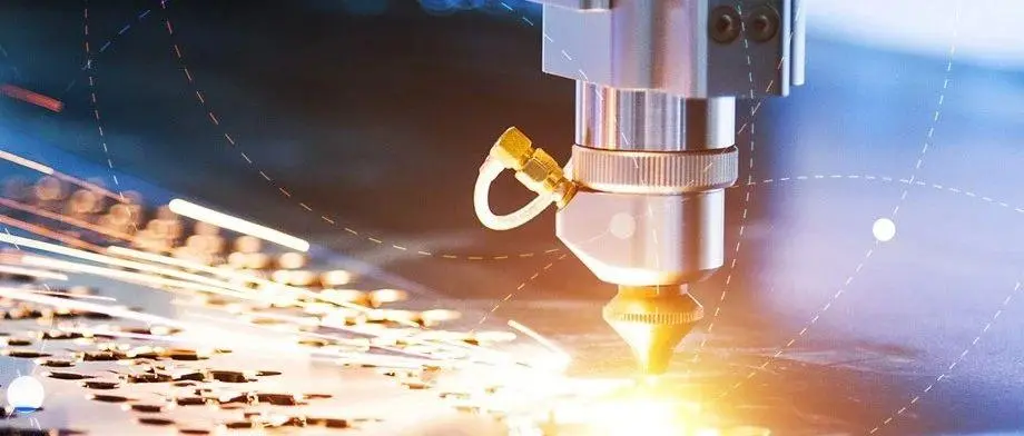
1. Principles and Advantages of Femtosecond Laser Ablation
Femtosecond lasers (10⁻¹⁵ s pulse width) enable nonlinear absorption (e.g., multiphoton ionization, avalanche ionization) with near-zero HAZ due to:
-
Non-thermal dominance: Energy deposition faster than heat diffusion (Cu thermal diffusion time≈1 ps);
-
High precision: SubmICron resolution (linewidth <5 μm), edge roughness Ra<0.1 μm;
-
Material versatility: Suitable for reflective metals (Cu), transparent materials, and composites.
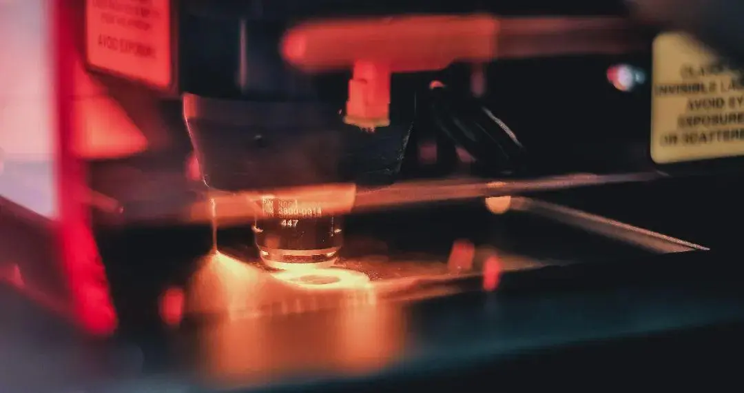
2. Key Process Parameters
(1) Laser Parameters
-
Wavelength: UV (343/515 nm) for higher Cu absorption (≈40% vs. IR 5%);
-
Pulse energy & fluence: 0.1–10 μJ/pulse, fluence=1–5 J/cm² (near Cu ablation threshold).
(2) Beam Control & Scanning
-
Focusing optics: High-NA objectives (NA≥0.5) for 1–5 μm spot size;
-
Scanning strategies: Spiral/raster scan, speed=1–10 m/s, ≤3 passes to minimize heat input.
(3) Environmental Control
-
Inert gas (Ar/N₂): Reduces oxidation (suRFace O<1 at.% via XPS);
-
Vacuum (<10⁻³ mbar): Suppresses plasma shielding.
3. Mechanisms for Zero HAZ
-
Electron-lattice decoupling: Energy confined to electrons, preventing thermal diffusion;
-
Phase explosion dominance: Direct sublimation/plasma formation avoids melting;
-
Heat accumulation suppression: Pulse interval (>10 ns) exceeds electron cooling time (≈1 ps).
4. Validation
-
Microscopy: SEM/TEM show no melting or lattice distortion (HAZ width <100 nm);
-
Chemical analysis: XPS confirms oxide thickness <2 nm; Raman shows no carbonization.
-
Functional tests:
-
Conductivity: Resistivity≈1.7 μΩ·cm (bulk-like);
-
Thermal stability: No HAZ growth after 300°C annealing.
-
5. Challenges & Solutions
-
Challenge 1: High reflectivity:
-
Solution: Anti-reflective coating (e.g., 10 nm Ti) or circular polarization.
-
-
Challenge 2: Plasma shielding:
-
Solution: Vacuum processing or lower repetition rate (<1 MHz).
-
-
Challenge 3: Low throughput:
-
Solution: Parallel multi-beam processing (DMD/SLM).
-
6. Applications & Economics
-
High-frequency PCBs: 28 GHz Antennas with <0.3 dB/cm loss;
-
Flexible electronics: PI-based Cu patterns withstand >10⁵ bends (R=1 mm);
-
Cost savings: 90% less chemical waste vs. lithography, 5× faster processing.