 PCB
PCB FPC
FPC Rigid-Flex
 FR-4
FR-4 HDI PCB
 Rogers High-Frequency Board
 PTFE Teflon High-Frequency Board
 Aluminum
 Copper Core
 PCB Assembly
 LED light PCBA
 Memory PCBA
 Power Supply PCBA
 New Energey PCBA
 Communication PCBA
 Industrial Control PCBA
 Medical Equipment PCBA
 Testing Service
 PCBA Testing Service
 Certification Application
 RoHS Certification Application
 REACH Certification Application
 CE Certification Application
 FCC Certification Application
 CQC Certification Application
 UL Certification Application
 Transformers, Inductors
 High Frequency Transformers
 Low Frequency Transformers
 High Power Transformers
 Conversion Transformers
 Sealed Transformers
 Ring Transformers
 Inductors
 Wires,Cables Customized
 Network Cables
 Power Cords
 Antenna Cables
 Coaxial Cables
 Net Position Indicator
 Solar AIS net position indicator
 Capacitors
 Connectors
 Diodes
 Embedded Processors & Controllers
 Digital Signal Processors (DSP/DSC)
 Microcontrollers (MCU/MPU/SOC)
 Programmable Logic Device(CPLD/FPGA)
 Communication Modules/IoT
 Resistors
 Through Hole Resistors
 Resistor Networks, Arrays
 Potentiometers,Variable Resistors
 Aluminum Case,Porcelain Tube Resistance
 Current Sense Resistors,Shunt Resistors
 Switches
 Transistors
 Power Modules
 Isolated Power Modules
 AC-DC Power Modules
 DC-AC Module(Inverter)
 RF and Wireless
Detailed Explanation of Special Processes for Microvia Processing in HDI Boards
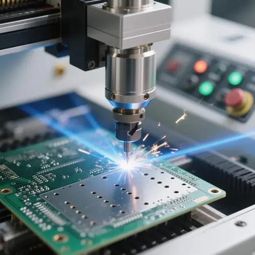
High-Density Interconnect (HDI) boards are critICal components for achieving miniaturization and high peRFormance in modern electronic devices. Their core lies in using microvias to achieve high-density interconnections between multiple layers. Microvias typically refer to blind or buried vias with a diameter of less than 0.15mm (6mil), and their processing quality directly determines the signal integrity and reliability of HDI boards. With the rapid development of 5G communication, artificial intelligence, and high-speed coMPUting equipment, the requirements for microvia processing accuracy are becoming increasingly stringent, driving innovation and application of a series of special processes. This article details the special processes used in microvia processing in HDI boards, such as laser drilling, electroplating filling, and lamination technology, and analyzes their technical difficulties and development trends.
1 Basic Concepts of HDI Boards and Microvias
HDI boards are known for their high circuit density and complex layered structure. Their core lies in achieving efficient electrical connections between multiple layers through micro blind and buried vias. A microvia (Microvia) is a tiny conductive via with a diameter usually less than 0.15mm, primarily used to connect different layers of a PCB, enabling stable electrical signal transmission under high-density wiring. Compared to traditional through-holes, microvias offer significant advantages:
-
Improved Signal Integrity: Reduced parasitic inductance and capacitance, optimizing high-speed signal transmission.
-
Optimized Wiring Density: Supports more compact circuit design, adapting to the needs of thin, light, short, and small devices.
-
Enhanced Electrical Performance: Reduced electromagnetic interference (EMI) and improved anti-interference capability.
-
Improved Structural Reliability: Reduced mechanical stress, enhanced resistance to vibration and thermal shock.
2 Laser Drilling Technology: The Core of High-Precision Microvia Formation
Laser drilling is the core process for creating micro blind and buried vias. Its non-contact, high-precision characteristics allow the aperture to be controlled to tens of micrometers, ensuring consistency in microvia size and smoothness of the hole wall, avoiding the rough hole walls and offset issues associated mechanical drilling.
2.1 Application Selection of UV Laser vs. CO2 Laser
-
UV Laser (Ultraviolet Laser): Concentrated energy, shorter wavelength, enabling smaller apertures (usually less than 50μm) and higher precision processing. UV lasers are particularly suitable for processing high-precision blind vias and ultra-thin materials, with smooth hole wall quality, but higher equipment and maintenance costs.
-
CO2 Laser: Relatively lower cost, suitable for processing microvias with larger apertures (usually greater than 75μm). However, its thermal effect is greater, potentially resulting rougher hole walls, often requiring post-processing to improve hole wall quality. For apertures between 50μm and 75μm, the choice between UV and CO2 laser can be based on actual precision and cost requirements.
2.2 Key Points of Laser Drilling Process Control
The quality of laser drilling depends on the precise control of numerous parameters:
-
Energy Density and Pulse Count: Require precise regulation to avoid excessive material ablation or incomplete drilling. For example, optimized process parameters for a 100μm micro blind via might be: pulse width 13.8μs, pulse energy 14.8mJ, pulses 2.
-
Focus Positioning: Ensures the laser beam is focused on the material surface for optimal drilling results and hole shape.
-
Material Adaptability: Different dielectric materials (e.g., FR-4, polyimide, Low-Dk materials) have different absorption rates for lasers, requiring adjusted laser parameters. Laser drilling has requirements for board materials; certain special materials may not be suitable.
Table: Characteristics Comparison of CO2 Laser vs. UV Laser in Microvia Processing
| Characteristic | CO2 Laser | UV Laser |
|---|---|---|
| Suitable Aperture Range | >75μm | <50μm |
| Processing Efficiency | High | Relatively High |
| Hole Wall Quality | Relatively rough, may require post-processing | Smooth, high quality |
| Equipment Cost | Relatively Low | High |
| Main Applications | Conventional HDI boards, larger aperture blind vias | High-end HDI, very small apertures, IC substrates |
3 Mechanical Drilling Technology: Application of Traditional Processes in Microvias
Although laser drilling has become mainstream, mechanical drilling still has applications in certain scenarios, particularly for buried vias and staggered blind via processes.
3.1 Technical Limitations and Challenges
Mechanical drilling is achieved through high-speed rotating tiny drill bits, but its lower aperture limit is constrained by drill bit manufacturing and machine tool accuracy, typically around 0.15mm. Smaller apertures easily lead to broken bits, excessive burrs, and other issues, causing a sharp decline in yield rate. Furthermore, the high hole wall roughness generated by mechanical drilling can pose plating challenges, making it difficult for the plating copper to completely fill the hole wall, potentially forming weak solder joints and causing overheating failures in high-current-density paths.
3.2 Micro-Drill Bit Technology and Process Optimization
To address these challenges, mechanical drilling uses ultra-fine drill bits (0.075mm-0.15mm) for microvia processing and is equipped with an automatic compensation system (Drill Bit Compensation) to maintain aperture stability. Optimizing drilling parameters, such as speed, feed rate, and drill point shape, is crucial for reducing burrs and improving hole wall quality.
4 Electroplating Filling Process: The Key to Ensuring Reliability of Electrical Connections
After microvia formation, metallization is essential to ensure the reliability of interlayer electrical connections. Electroplating filling is the core process of this step, and its quality directly affects the conduction performance and long-term reliability.
4.1 Electroless Copper Deposition
Microvia metallization first requires electroless copper deposition (also known as chemical copper plating) on the hole wall to form a uniform conductive layer. The key to this process is ensuring the hole wall is sufficiently activated and that the copper layer covers evenly, even in deep holes.
4.2 Electroplating Copper Filling
After electroless copper deposition, the copper layer is thickened through electroplating to enhance conductivity and mechanical strength. The goal of electroplating filling is to achieve void-free plating, avoiding signal transmission interruption or reliability degradation.
-
Plating Solution Additives: Using plating solutions containing additives like leveling agents and brighteners can improve the uniform deposition ability of copper within microvias, preventing voids or uneven plating.
-
Current Density Control: Adopting combined electroplating process parameters is an effective method to improve filling efficiency and quality. Research shows that using a stepped current density (e.g., 1.8A/dm²×15min + 1.0A/dm²×30min + 1.8A/dm²×15min) can achieve a high filling rate (96.1%) while shortening plating time. Low current density offers high filling rate but is time-consuming, while high current density saves time but is prone to voids.
-
Uniformity Control: Advanced electroplating technologies require the uniformity of electroplated copper thickness to be controlled within ±5% to ensure conductive reliability and impedance consistency.
5 Lamination Technology: The Foundation for Realizing Multi-layer Microvia Structures
HDI boards typically employ a multiple lamination structure, with blind and buried vias formed through multiple lamination processes1. Lamination quality directly affects the stability and electrical performance of the microvia structure.
5.1 Vacuum Lamination Technology
Vacuum lamination technology is widely used. It can remove air between layers, improve lamination quality, ensure stable electrical connections between layers in multi-stage structures, and maintain the flatness and mechanical stability of the entire PCB board. This is crucial for preventing layer separation and hole wall deformation.
5.2 Precise Parameter Control
During the lamination process, parameters such as temperature, pressure, and time need to be precisely controlled. Improper control can lead to uneven resin flow, microvia deformation, or layer separation, affecting electrical performance and mechanical strength. The matching of the mechanical properties and coefficient of thermal expansion (CTE) of materials is also an important factor in preventing layer delamination and warping.
6 Quality Control and Inspection: Ensuring the Precision of Microvia Processing
Due to the complex structure of HDI, microvia processing quality relies on a variety of precision inspection methods to ensure.
-
Automated Optical Inspection (AOI): Used to detect the positional accuracy of microvias, surface defects, and circuit integrity.
-
X-Ray Inspection: A non-destructive testing method particularly suitable for inspecting the connectivity of blind and buried vias, interlayer bonding condition, and internal void defects in electroplated fills. X-ray can also detect the quality of microvias under BGA solder balls.
-
Flying Probe Test: Mainly used to verify electrical connectivity and check for electrical defects such as open or short circuits in microvias.
-
Metallographic Sectioning Analysis: The gold standard for destructive analysis. By cutting, polishing, and microscopic examination, the hole shape, copper plating thickness, uniformity, and the presence of defects such as voids or cracks can be precisely observed. This is an important means for process validation and failure analysis.
7 Considerations for Material Selection in Microvia Processing
The choice and effectiveness of microvia processing techniques are closely related to the materials used. HDI boards have special requirements for materials:
-
Dielectric Materials: Need to possess low dielectric constant (Dk) and low dissipation factor (Df) to reduce loss and delay during high-speed signal transmission. Simultaneously, materials also need to have high thermal stability to reduce thermal expansion mismatch and prevent delamination or warping during processing.
-
Copper Foil: The use of ultra-thin copper foil (e.g., ≤12μm) helps achieve finer circuit fabrication.
-
Other High-Performance Materials: For high-frequency applications, high-performance materials such as PTFE (polytetrafluoroethylene) may be used, but these materials often pose additional challenges for laser drilling and lamination.
8 Development Trends in Microvia Processing Technology
Microvia processing technology continues to evolve to meet the increasing demands of electronic products:
-
Higher Density Interconnection: Apertures continue to shrink, developing towards below 50μm and even smaller. The application of stacked microvias and staggered microvias technology is increasing to achieve higher density interconnections.
-
Advanced Integration Technologies: Embedded components, 3D printed electronics, system-in-package (SiP) and other technologies will be more closely integrated with HDI microvia processes.
-
Material Innovation: New low Dk/Df materials, high-temperature resistant materials, and environmentally friendly materials will continue to emerge, driving corresponding adjustments and developments in microvia processing technology.
-
Intelligence and Automation: Utilizing artificial intelligence (AI) and machine learning (ML) to optimize drilling parameters, predict product quality, and achieve intelligent manufacturing will be key to improving yield and efficiency.