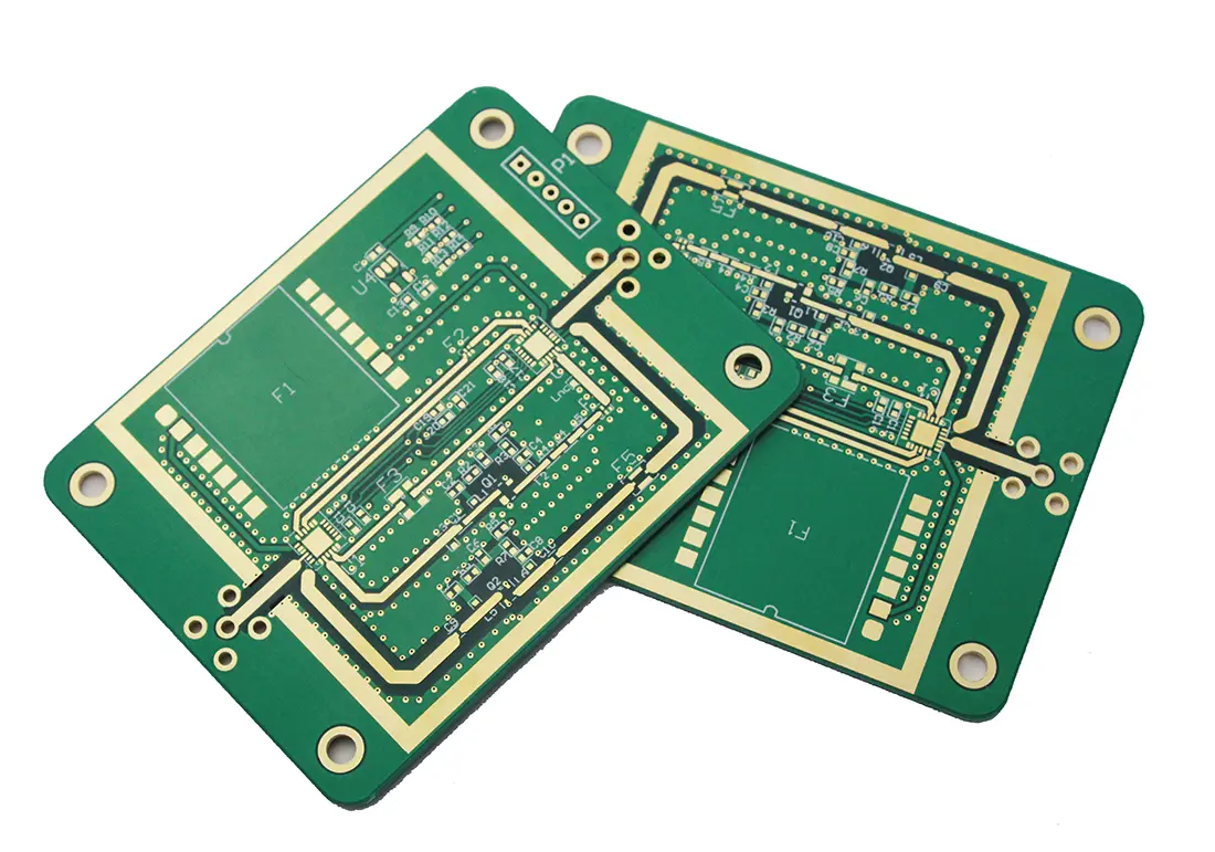
 PCB
PCB FPC
FPC Rigid-Flex
 FR-4
FR-4 HDI PCB
 Rogers High-Frequency Board
 PTFE Teflon High-Frequency Board
 Aluminum
 Copper Core
 PCB Assembly
 LED light PCBA
 Memory PCBA
 Power Supply PCBA
 New Energey PCBA
 Communication PCBA
 Industrial Control PCBA
 Medical Equipment PCBA
 Testing Service
 PCBA Testing Service
 Certification Application
 RoHS Certification Application
 REACH Certification Application
 CE Certification Application
 FCC Certification Application
 CQC Certification Application
 UL Certification Application
 Transformers, Inductors
 High Frequency Transformers
 Low Frequency Transformers
 High Power Transformers
 Conversion Transformers
 Sealed Transformers
 Ring Transformers
 Inductors
 Wires,Cables Customized
 Network Cables
 Power Cords
 Antenna Cables
 Coaxial Cables
 Net Position Indicator
 Solar AIS net position indicator
 Capacitors
 Connectors
 Diodes
 Embedded Processors & Controllers
 Digital Signal Processors (DSP/DSC)
 Microcontrollers (MCU/MPU/SOC)
 Programmable Logic Device(CPLD/FPGA)
 Communication Modules/IoT
 Resistors
 Through Hole Resistors
 Resistor Networks, Arrays
 Potentiometers,Variable Resistors
 Aluminum Case,Porcelain Tube Resistance
 Current Sense Resistors,Shunt Resistors
 Switches
 Transistors
 Power Modules
 Isolated Power Modules
 AC-DC Power Modules
 DC-AC Module(Inverter)
 RF and Wireless
Enhancing Electroless Copper Adhesion on PTFE Substrates via Cold Plasma Treatment
1. PTFE Surface Challenges
PTFE’s low surface energy (18–24 mN/m) and chemICal inertness lead to:
-
Weak adhesion: Lack of functional groups for chemical bonding;
-
Poor wettability: Contact angle >110°;
-
CTE mismatch: PTFE (100–150 ppm/°C) vs. Cu (17 ppm/°C) causes delamination.
2. Cold Plasma Mechanism
Cold plasma modifies PTFE via:
-
Physical etching: Increases roughness (Ra: 0.1→0.5–2 μm);
-
Chemical activation: Introduces polar groups (-C=O, -COOH, -NH₂), raising surface energy to 50–70 mN/m;
-
Cross-linking: Enhances mechanical interlocking.
3. Process Optimization
(1) Plasma Parameters
-
Gases:
-
O₂: Maximizes oxygen-containing groups (O/C ratio: 0.02→0.3);
-
N₂/H₂ (4:1): Generates -NH₂ for Pd catalyst bonding;
-
Ar: Pre-cleaning via physical etching.
-
-
Conditions:
-
Power: 50–300 W;
-
Time: 30–180 s;
-
Pressure: 10–100 Pa;
-
Electrode gap: 5–20 mm.
-
(2) Post-Treatment Stability
-
Modified surfaces degrade by ~30% in 24 hours; N₂ storage extends activity to 48 hours.
4. Electroless Copper Process
(1) Activation
-
Pd activation: PdCl₂/SnCl₂ colloid (50–100 ppm Pd), >90% coverage (XPS).
(2) Plating -
Bath composition:
-
CuSO₄ (10–20 g/L);
-
Reducer: Formaldehyde (5–10 mL/L) or NaH₂PO₂ (20–30 g/L);
-
EDTA (30–50 g/L); pH 12.5–13.5.
-
-
Conditions: 40–60°C for 20–60 min (1–5 μm Cu thickness).
5. Adhesion Validation
-
Surface characterization:
-
Contact angle: <30° post-treatment;
-
XPS: O/C=0.3, N/C=0.1 (N₂/H₂);
-
AFM/SEM: Ra=1.5 μm.
-
-
Adhesion tests:
-
Peel strength: 1.5–2.5 N/mm (ASTM D3359);
-
Thermal shock: No delamination after 1000 cycles (-55–125°C).
-
6. Challenges & Solutions
-
Challenge 1: Non-uniform modification:
-
Solution: Rotating sample holders/multi-electrode arrays.
-
-
Challenge 2: Poor bath penetration:
-
Solution: Vacuum-assisted impregnation.
-
-
Challenge 3: Environmental stability:
-
Solution: Silane coupling agents (e.g., APTES) or plasma-polymerized coatings.
-
7. Applications & Economics
-
High-frequency PCBs: 2.0 N/mm adhesion, <0.2 dB/mm loss @28 GHz;
-
Flexible circuits: Withstands 100k bends (R=5 mm);
-
Cost savings: 50% lower waste treatment costs vs. chemical etching.