 PCB
PCB FPC
FPC Rigid-Flex
 FR-4
FR-4 HDI PCB
 Rogers High-Frequency Board
 PTFE Teflon High-Frequency Board
 Aluminum
 Copper Core
 PCB Assembly
 LED light PCBA
 Memory PCBA
 Power Supply PCBA
 New Energey PCBA
 Communication PCBA
 Industrial Control PCBA
 Medical Equipment PCBA
 Testing Service
 PCBA Testing Service
 Certification Application
 RoHS Certification Application
 REACH Certification Application
 CE Certification Application
 FCC Certification Application
 CQC Certification Application
 UL Certification Application
 Transformers, Inductors
 High Frequency Transformers
 Low Frequency Transformers
 High Power Transformers
 Conversion Transformers
 Sealed Transformers
 Ring Transformers
 Inductors
 Wires,Cables Customized
 Network Cables
 Power Cords
 Antenna Cables
 Coaxial Cables
 Net Position Indicator
 Solar AIS net position indicator
 Capacitors
 Connectors
 Diodes
 Embedded Processors & Controllers
 Digital Signal Processors (DSP/DSC)
 Microcontrollers (MCU/MPU/SOC)
 Programmable Logic Device(CPLD/FPGA)
 Communication Modules/IoT
 Resistors
 Through Hole Resistors
 Resistor Networks, Arrays
 Potentiometers,Variable Resistors
 Aluminum Case,Porcelain Tube Resistance
 Current Sense Resistors,Shunt Resistors
 Switches
 Transistors
 Power Modules
 Isolated Power Modules
 AC-DC Power Modules
 DC-AC Module(Inverter)
 RF and Wireless
Minintel Technology: Elevating PCB/PCBA Quality Standards with Advanced X-Ray Inspection in Shenzhen
2026-01-11
Nestled in the heart of Shenzhen’s bustling electronics manufacturing hub—known globally as the “Silicon Valley of Hardware”—Minintel Technology Co., Ltd. stands as a beacon of precision, reliability, and innovation in the PCB (Printed Circuit Board) and PCBA (Printed Circuit Board Assembly) industry. For over a decade, Minintel has dedicated itself to delivering professional and efficient PCB and PCBA services, catering to clients across aerospace, automotive, medical technology, industrial control, and consumer electronics sectors worldwide. What sets Minintel apart in this highly competitive lanDSCape is its unwavering commitment to quality assurance, anchored by cutting-edge non-destructive testing (NDT) technologies—most notablyPCB x-ray, PCBA x-ray, and comprehensive x-ray inspection solutions. By integrating state-of-the-art x ray inspectioninto every stage of production, Minintel ensures that every product leaving its Shenzhen facility meets the most stringent quality standards, reinforcing its reputation as a trusted partner for businesses that refuse to compromise on peRFormance or reliability.
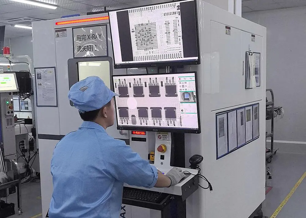
The Critical Role of X-Ray Inspection in Modern PCB/PCBA Manufacturing
In the era of miniaturized electronics and complex circuit designs, traditional quality control methods—such as visual inspection with the naked eye or automated optical inspection (AOI)—are no longer sufficient to detect all potential defects. As PCBs evolve to feature finer pitch components, higher layer counts, and buried vias, and as PCBA assemblies incorporate tiny surface-mount technology (SMT) components (some as small as 01005) and dense solder joints, defects often lurk beneath the surface, invisible to conventional inspection tools. This is where x-ray inspection emerges as an indispensable quality control tool, and Minintel has recognized its transformative potential since its inception.
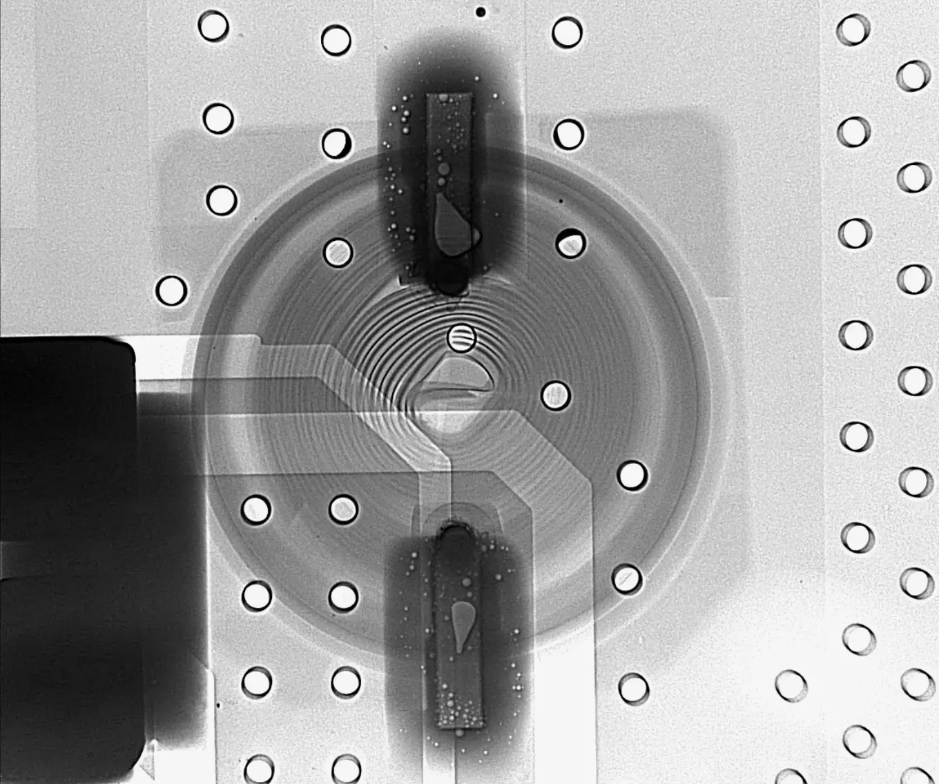
X ray inspection works on the principle of penetrating radiation, which passes through the PCB or PCBA and creates a detailed image of internal structures based on differences in material density. Metals (such as copper traces, solder joints, and component leads) absorb more X-rays, appearing as dark areas in the image, while non-metallic materials (such as FR-4 substrates or plastic components) allow more radiation to pass through, appearing lighter. This capability enables inspectors to visualize internal defects that would otherwise go undetected, including solder bridging, voids, cold joints, insufficient solder, misaligned components, and even internal layer separations in PCBs.
For Minintel, which serves industries where product failure can have catastrophic consequences—such as medical devices that directly impact patient safety, automotive electronics that influence vehicle performance, or aerospace components that operate in extreme environments—x-ray inspection is not just a quality control measure but a moral and professional obligation. The company’s investment in PCB x-ray and PCBA x-ray technology reflects its understanding that in modern electronics manufacturing, quality is not an add-on but a foundational element of every service it provides.
Minintel’s X-Ray Inspection Ecosystem: From PCB to PCBA
Minintel’s quality control laboratory in Shenzhen is a testament to its commitment to technological excellence. The facility houses a fleet of advanced X-ray inspection systems, each tailored to address the unique quality challenges of PCB manufacturing and PCBA assembly. By separating PCB x-ray and PCBA x-ray capabilities, Minintel ensures that each stage of production receives specialized inspection that aligns with its specific requirements, delivering unparalleled accuracy and reliability.
PCB X-Ray: Ensuring Structural Integrity from Layer 1 to Layer N
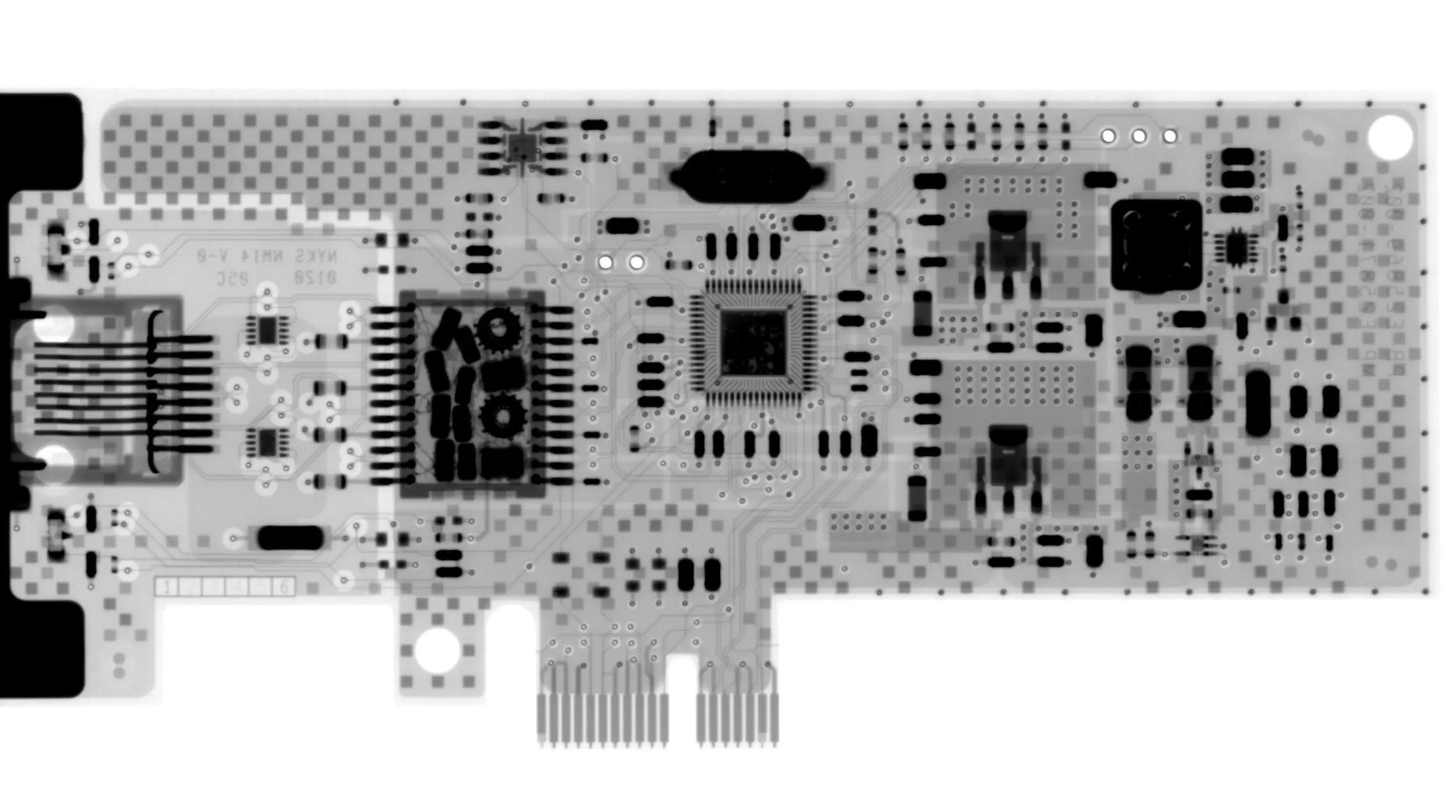
PCBs are the backbone of all electronic devices, and their structural integrity directly impacts the performance and lifespan of the final product. Minintel’s PCB x-ray systems are designed to inspect the internal structure of bare PCBs, identifying defects that occur during fabrication—many of which are invisible to the naked eye or standard AOI systems.
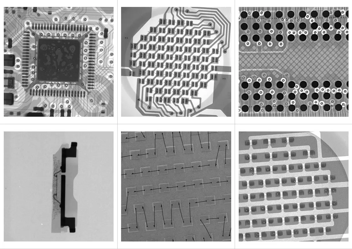
One of the primary applications of PCB x-ray at Minintel is the inspection of buried and blind vias. Buried vias (which connect internal layers without reaching the board surface) and blind vias (which connect an outer layer to one or more internal layers) are critical for high-density PCBs, but their fabrication is prone to defects such as incomplete plating, voids, or misalignment. Using x ray inspection, Minintel’s quality control team can verify that vias are properly formed, fully plated, and free of air bubbles or contaminants that could impede electrical conductivity. For example, a void in a via can increase resistance, leading to overheating and eventual failure—especially in high-power applications. PCB x-ray allows Minintel to detect such defects early in the production process, preventing costly rework or product recalls down the line.
Another key use case for PCB x-ray is the inspection of internal layer alignment. Multi-layer PCBs (ranging from 2-layer to 24-layer designs at Minintel) require precise alignment of each layer during lamination to ensure that conductive traces line up correctly. Even a slight misalignment (measured in micrometers) can cause short circuits or open circuits, rendering the PCB unusable. X ray inspection provides a cross-sectional view of the PCB, allowing inspectors to measure layer registration with micron-level accuracy and ensure compliance with client specifications.
Minintel’s PCB x-ray systems also play a crucial role in inspecting copper thickness and trace integrity. Copper traces are the pathways for electrical signals, and variations in thickness or breaks in the trace can compromise signal transmission. Using x ray inspection, the company can verify that copper traces meet the required thickness (from 1oz to 4oz and beyond) and are free of cracks, scratches, or thinning—defects that could lead to signal degradation or intermittent failures.
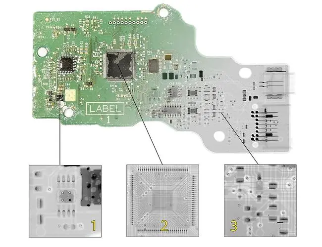
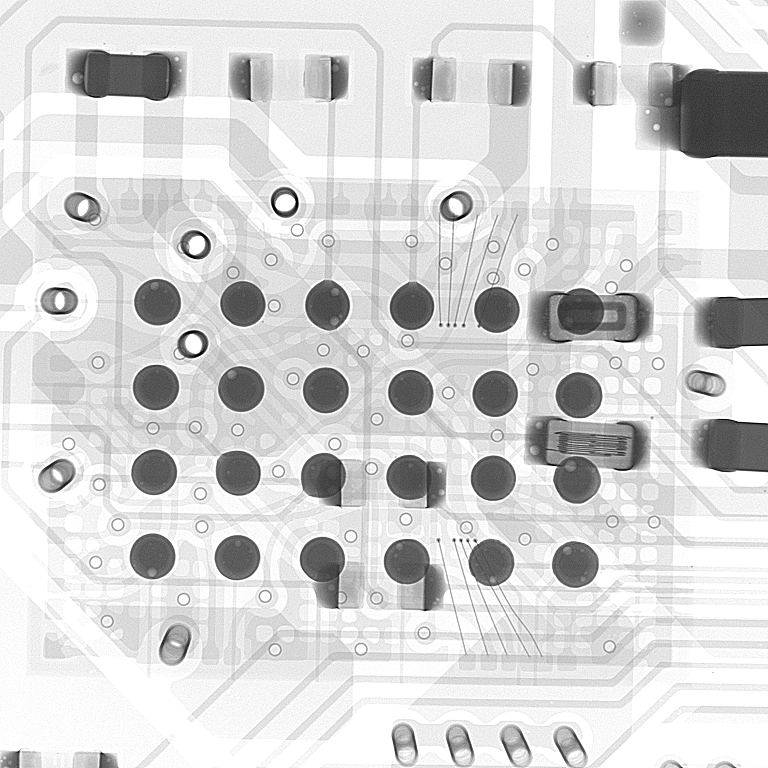
PCBA X-Ray: Securing Solder Joint Quality and Component Placement
Once a bare PCB passes PCB x-ray inspection, it moves to the PCBA assembly line, where components are soldered onto the board. This stage introduces new quality challenges, as solder joints and component placement are prone to defects that can only be reliably detected with PCBA x-ray technology.
Solder joint defects are among the most common issues in PCBA assembly, and PCBA x-ray is the gold standard for detecting them. Minintel’s PCBA x-ray systems can identify a wide range of solder joint defects, including:
- Voids: Air bubbles trapped in the solder, which reduce mechanical strength and thermal conductivity. Voids exceeding 25% of the solder joint area are typically considered critical, as they can lead to premature failure under thermal cycling or vibration.
- Solder bridging: Unintended connections between adjacent solder pads, which cause short circuits. This is particularly common in fine-pitch components such as BGAs (Ball Grid Arrays) and QFPs (Quad Flat Packs), where pad spacing is as small as 0.4mm.
- Insufficient solder: Too little solder on the joint, leading to poor electrical contact and mechanical stability.
- Cold joints: Solder that did not properly melt during reflow, resulting in a brittle, unreliable connection.
- Tombstoning: Components that lift off the PCB on one end, caused by uneven solder wetting.
BGAs and other area-array packages are a particular focus of PCBA x-ray inspection at Minintel. These components have solder balls underneath the package, which are completely hidden from view once the component is mounted. Without x ray inspection, it is impossible to verify the quality of these solder joints. Minintel’s PCBA x-ray systems use 3D imaging technology to capture detailed views of each solder ball, allowing inspectors to check for voids, bridging, and proper wetting. This is especially critical for medical and automotive applications, where BGA failures can lead to life-threatening consequences.
Component placement accuracy is another area where PCBA x-ray excels. Even with high-speed pick-and-place machines, components can be misaligned, rotated, or missing. X ray inspection allows Minintel to verify that components are placed within the specified tolerance (typically ±0.1mm for most components) and that no critical components are missing. For tiny 01005 components, which are smaller than a grain of rice, PCBA x-ray provides the resolution needed to detect even minor placement errors that could affect the functionality of the assembly.
The Technology Behind Minintel’s X-Ray Inspection Systems
Minintel’s commitment to quality is reflected in its investment in the latest x-ray inspection technology. The company’s Shenzhen facility is equipped with a range of advanced X-ray systems from leading global manufacturers, including 2D X-ray inspectors, 3D computed tomography (CT) X-ray systems, and automated inline X-ray inspection machines. Each system is selected for its specific capabilities, ensuring that Minintel can address the quality needs of every client, regardless of product complexity or volume.
2D X-Ray Inspection: Speed and Efficiency for High-Volume Production
For high-volume production lines, Minintel uses automated inline 2D x ray inspection systems that integrate seamlessly into the manufacturing process. These systems can inspect up to 60 PCBs or PCBAs per hour, providing real-time feedback to production teams and allowing for immediate adjustments if defects are detected. The 2D systems use high-resolution cameras and advanced image processing software to identify defects, with programmable inspection algorithms tailored to specific product designs. This automation ensures consistency in inspection results, eliminating human error and reducing inspection time without compromising accuracy.
3D CT X-Ray Inspection: Precision for Complex Designs
For complex products—such as high-density HDI PCBs, multi-layer PCBs with buried vias, or PCBA assemblies with BGAs and other area-array components—Minintel relies on 3D CT x-ray inspection systems. These systems use computed tomography technology to create detailed 3D models of the PCB or PCBA, allowing inspectors to visualize internal structures from any angle and measure defects with micron-level precision.
3D CT x ray inspection is particularly valuable for root cause analysis. When a defect is detected, the 3D model allows Minintel’s engineering team to examine the defect in three dimensions, determining its exact location, size, and cause. For example, if a via is found to have a void, the 3D model can show whether the void was caused by improper plating, contamination during fabrication, or another issue. This information is critical for continuous improvement, as it allows Minintel to address the root cause and prevent similar defects from occurring in future production runs.
Advanced Software Integration: Data-Driven Quality Control
Minintel’s x-ray inspection systems are not just hardware—they are part of a comprehensive data-driven quality control ecosystem. The inspection systems are integrated with the company’s Manufacturing Execution System (MES) and Quality Management System (QMS), allowing for real-time data collection, analysis, and reporting. Every PCB x-ray and PCBA x-ray inspection generates a detailed report, including images of the product, defect locations, and measurements. This data is stored in a centralized database, where it can be accessed by production teams, engineers, and clients.
For clients, this means complete transparency into the quality control process. Minintel provides detailed inspection reports with every order, allowing clients to verify that their products meet the specified quality standards. The data also enables Minintel to track quality trends over time, identifying areas for improvement and implementing corrective actions proactively. For example, if the data shows an increase in solder voids in a particular product line, the engineering team can adjust the reflow soldering parameters or component sourcing to address the issue.
X-Ray Inspection in Minintel’s Quality Assurance Workflow
At Minintel, x-ray inspection is not an afterthought—it is integrated into every stage of the PCB and PCBA manufacturing process, from incoming material inspection to final product testing. This proactive approach ensures that defects are detected early, reducing rework costs, shortening lead times, and ensuring that only high-quality products reach clients.
Stage 1: Incoming Material Inspection
Before any raw materials are used in production, they undergo rigorous inspection—including x ray inspection for critical components. Minintel’s quality control team uses PCBA x-ray systems to inspect incoming components such as BGAs, CSPs (Chip Scale Packages), and connectors, verifying that they are free of defects such as damaged solder balls, internal cracks, or counterfeit components. This step is crucial for preventing defects that could be introduced by faulty materials, ensuring that the production process starts with high-quality inputs.
Stage 2: PCB Fabrication Inspection
During PCB fabrication, PCB x-ray inspection is performed at key checkpoints:
- After drilling: To verify that holes are properly sized, positioned, and free of burrs.
- After plating: To inspect via plating quality, ensuring that vias are fully plated and free of voids.
- After lamination: To check layer alignment and detect internal delaminations.
- Final bare PCB inspection: A comprehensive x ray inspection to ensure that the finished PCB meets all structural and electrical specifications.
Stage 3: PCBA Assembly Inspection
PCBA assembly involves multiple inspection steps, with PCBA x-ray playing a central role:
- After component placement: To verify that components are correctly positioned before soldering.
- After reflow soldering: To inspect solder joint quality, including voids, bridging, and insufficient solder.
- After wave soldering: For through-hole components, to ensure proper solder penetration and joint quality.
- Final PCBA inspection: A comprehensive x ray inspection to ensure that the assembled board is free of defects and ready for functional testing.
Stage 4: Functional Testing and Final Verification
After x-ray inspection, all PCBAs undergo functional testing to verify that they perform as intended. However, x ray inspection remains a critical backup—if a PCB fails functional testing, Minintel’s engineers can use PCBA x-ray to examine the board and identify the root cause of the failure, whether it is a solder joint defect, component misalignment, or another issue. This reduces troubleshooting time and allows for faster rework, ensuring that clients receive their orders on time.
Case Studies: How X-Ray Inspection Delivers Value for Minintel’s Clients
Minintel’s investment in PCB x-ray, PCBA x-ray, and x-ray inspection has not only elevated its own quality standards but has also delivered tangible value for clients across industries. Here are three examples of how x ray inspection has helped Minintel’s clients overcome quality challenges and achieve their business goals:
Case Study 1: Medical Device Manufacturer
A leading medical device manufacturer approached Minintel to produce PCBs and PCBAs for a portable cardiac monitor. The product required high reliability, as failures could put patients at risk, and it needed to comply with strict FDA and ISO 13485 standards. The PCBA included a BGA component with a 0.5mm pitch, which was critical for the monitor’s signal processing capabilities.
During initial production, Minintel’s PCBA x-ray system detected solder voids in 5% of the BGA joints—just below the client’s maximum allowable limit of 6%. While the voids were not critical, Minintel’s engineering team used 3D CT x ray inspection to analyze the root cause, discovering that the voids were due to a slight inconsistency in the reflow soldering temperature profile. The team adjusted the temperature settings, and subsequent PCBA x-ray inspections showed that voids were reduced to less than 1%.
The client was impressed by Minintel’s proactive approach and the detailed data provided by the x-ray inspection reports. “We rely on Minintel not just for manufacturing, but for quality assurance,” said the client’s engineering director. “The PCBA x-ray inspections give us the confidence that our products are safe and reliable, which is essential in the medical industry.” Today, the portable cardiac monitor is used in hospitals across 30 countries, and Minintel remains the exclusive PCB/PCBA supplier for the product line.
Case Study 2: Automotive Electronics Supplier
An automotive electronics supplier partnered with Minintel to produce PCBs for advanced driver-assistance systems (ADAS). ADAS components operate in harsh environments—exposed to extreme temperatures, vibration, and electromagnetic interference—and require zero defects. The PCBs featured 12 layers with buried vias and blind vias, making them particularly complex to manufacture.
Minintel’s PCB x-ray system played a critical role in ensuring the structural integrity of the PCBs. During inspection, the system detected a small misalignment between two internal layers in a batch of 500 PCBs. The misalignment was less than 50 microns, which would have been undetectable with traditional inspection methods, but it could have led to short circuits under the stress of automotive operation. Minintel immediately quarantined the batch, reworked the affected PCBs, and adjusted the lamination process to prevent future misalignments.
The client’s quality manager noted, “ADAS systems leave no room for error. Minintel’s PCB x-ray inspection caught a defect that would have caused costly recalls and potentially dangerous failures. Their commitment to quality has saved us millions of dollars and protected our reputation.” Since then, the client has expanded its partnership with Minintel to include PCBA assembly services, citing the company’s advanced x ray inspection capabilities as a key reason for the expansion.
Case Study 3: Industrial Control Equipment Manufacturer
A manufacturer of industrial control systems needed a reliable partner to produce PCBs and PCBAs for its programmable logic controllers (PLCs). The PLCs are used in manufacturing facilities to control critical processes, and downtime due to equipment failure can cost clients thousands of dollars per hour. The PCBA included a mix of SMT and through-hole components, with tight tolerance requirements for component placement.
During high-volume production, Minintel’s inline 2D x ray inspection system detected a trend of solder bridging between two adjacent pads on a QFP component. The bridging was caused by a slight deviation in the pick-and-place machine’s calibration, which had gone unnoticed in visual inspections. Minintel’s production team adjusted the machine’s calibration within hours, and the x ray inspection system verified that the bridging issue was resolved.
The client’s operations director commented, “Minintel’s automated x-ray inspection system allowed them to detect and resolve a quality issue before it affected a large number of products. This level of efficiency and attention to detail is exactly what we need in a manufacturing partner. Thanks to their PCBA x-ray capabilities, our PLCs have a failure rate of less than 0.01%, which is well below industry averages.”
Minintel’s Commitment to Continuous Improvement in X-Ray Inspection
In the fast-paced electronics industry, technology evolves rapidly, and Minintel is committed to staying at the forefront of x-ray inspection innovation. The company invests heavily in research and development, regularly updating its X-ray systems and software to keep pace with emerging trends in PCB/PCBA design and manufacturing.
One area of focus is the integration of artificial intelligence (AI) and machine learning into x ray inspection processes. Minintel is currently piloting AI-powered PCB x-ray and PCBA x-ray systems that can learn from historical inspection data to identify defects more accurately and efficiently. These systems use algorithms to recognize patterns in defect images, reducing false positives and improving inspection speed. For example, the AI system can distinguish between a harmless air bubble and a critical void in a solder joint, reducing the need for manual review and speeding up the inspection process.
Another area of investment is the expansion of 3D CT x-ray inspection capabilities. As PCBs and PCBAs become more complex, 3D imaging will play an increasingly important role in quality control. Minintel plans to add additional 3D CT systems to its Shenzhen facility, allowing for faster and more detailed inspection of complex products.
Minintel also places a strong emphasis on training its quality control team to maximize the effectiveness of x-ray inspection technology. All inspectors undergo rigorous training on X-ray system operation, defect identification, and image analysis, and they receive regular updates on new technologies and industry best practices. This ensures that Minintel’s team can leverage the full capabilities of the X-ray systems, delivering consistent and reliable inspection results.
Sustainability and Safety in X-Ray Inspection
Minintel recognizes that advanced technology must be balanced with environmental responsibility and employee safety. The company’s x-ray inspection systems are designed to be energy-efficient, with low power consumption and standby modes that reduce energy use when not in operation. Additionally, Minintel has implemented a comprehensive waste reduction program, recycling packaging materials and electronic waste from the inspection systems.
Employee safety is a top priority at Minintel. All PCB x-ray and PCBA x-ray systems are equipped with advanced safety features, including lead shielding, interlock systems that prevent access to the X-ray beam during operation, and radiation monitoring devices. The company’s safety team conducts regular inspections of the X-ray systems to ensure compliance with international radiation safety standards, and all employees who work with the systems receive specialized training on radiation safety.
Why Choose Minintel for PCB/PCBA Services with Advanced X-Ray Inspection?
For businesses seeking a reliable PCB/PCBA manufacturing partner in Shenzhen, Minintel Technology Co., Ltd. offers a unique combination of expertise, technology, and commitment to quality—all anchored by its advanced x-ray inspection capabilities. Here are the key reasons why clients around the world choose Minintel:
1. Uncompromising Quality Assurance
Minintel’s integration of PCB x-ray, PCBA x-ray, and x ray inspection into every stage of production ensures that every product meets the highest quality standards. The company’s zero-defect policy for critical applications and compliance with international standards (ISO 9001, ISO 13485, IATF 16949) provide clients with the confidence that their products are reliable and fit for purpose.
2. Advanced Technology and Innovation
Minintel’s investment in the latest X-ray inspection systems—including 2D inline inspectors, 3D CT systems, and AI-powered technology—ensures that the company can address the quality needs of even the most complex products. The company’s commitment to continuous improvement means that clients benefit from the latest advancements in quality control technology.
3. Professional and Efficient Service
As a Shenzhen-based manufacturer, Minintel leverages the city’s robust supply chain and manufacturing ecosystem to deliver fast lead times and competitive pricing. The company’s team of engineers and technicians has extensive experience in PCB/PCBA manufacturing, and they work closely with clients to understand their needs and provide customized solutions.
4. Transparency and Accountability
Minintel’s data-driven quality control system provides clients with complete transparency into the inspection process. Detailed x-ray inspection reports allow clients to verify quality, and the company’s proactive approach to defect prevention ensures that issues are addressed before they affect production.
5. Industry-Specific Expertise
Minintel has deep experience serving clients in aerospace, automotive, medical technology, industrial control, and consumer electronics. The company’s team understands the unique quality requirements of each industry and tailors its x ray inspection processes to meet those needs.
Minintel—Where Precision Meets Trust in Shenzhen’s Electronics Hub
In Shenzhen’s dynamic electronics manufacturing landscape, Minintel Technology Co., Ltd. has established itself as a leader in PCB and PCBA services, driven by its unwavering commitment to quality and innovation. The company’s investment in PCB x-ray, PCBA x-ray, and x-ray inspection technology is a testament to its understanding that quality is the foundation of long-term success in the electronics industry.
By integrating advanced x ray inspection into every stage of production, Minintel ensures that its clients receive products that are reliable, durable, and fit for purpose—whether they are used in life-saving medical devices, critical automotive systems, or cutting-edge consumer electronics. The company’s Shenzhen facility, with its state-of-the-art quality control laboratory and team of skilled professionals, is a hub of precision and efficiency, delivering professional PCB/PCBA services that meet the needs of clients worldwide.
As the electronics industry continues to evolve—with smaller components, more complex designs, and higher quality expectations—Minintel remains committed to staying at the forefront of x-ray inspection technology. The company’s focus on continuous improvement, sustainability, and client satisfaction ensures that it will remain a trusted partner for businesses seeking to thrive in the global electronics market.
For businesses looking for a PCB/PCBA manufacturing partner in Shenzhen that combines technical expertise, advanced technology, and a relentless focus on quality, Minintel Technology Co., Ltd. is the clear choice. With Minintel, you can be confident that your products are backed by the best x ray inspection technology available, delivering the precision and reliability that your business deserves. In the world of electronics manufacturing, where every detail matters, Minintel is more than a supplier—it’s a strategic partner dedicated to your success.