 PCB
PCB FPC
FPC Rigid-Flex
 FR-4
FR-4 HDI PCB
 Rogers High-Frequency Board
 PTFE Teflon High-Frequency Board
 Aluminum
 Copper Core
 PCB Assembly
 LED light PCBA
 Memory PCBA
 Power Supply PCBA
 New Energey PCBA
 Communication PCBA
 Industrial Control PCBA
 Medical Equipment PCBA
 Testing Service
 PCBA Testing Service
 Certification Application
 RoHS Certification Application
 REACH Certification Application
 CE Certification Application
 FCC Certification Application
 CQC Certification Application
 UL Certification Application
 Transformers, Inductors
 High Frequency Transformers
 Low Frequency Transformers
 High Power Transformers
 Conversion Transformers
 Sealed Transformers
 Ring Transformers
 Inductors
 Wires,Cables Customized
 Network Cables
 Power Cords
 Antenna Cables
 Coaxial Cables
 Net Position Indicator
 Solar AIS net position indicator
 Capacitors
 Connectors
 Diodes
 Embedded Processors & Controllers
 Digital Signal Processors (DSP/DSC)
 Microcontrollers (MCU/MPU/SOC)
 Programmable Logic Device(CPLD/FPGA)
 Communication Modules/IoT
 Resistors
 Through Hole Resistors
 Resistor Networks, Arrays
 Potentiometers,Variable Resistors
 Aluminum Case,Porcelain Tube Resistance
 Current Sense Resistors,Shunt Resistors
 Switches
 Transistors
 Power Modules
 Isolated Power Modules
 AC-DC Power Modules
 DC-AC Module(Inverter)
 RF and Wireless
Detailed Explanation of Materials and Processes for Component Lead Plating
Part One: Detailed Explanation of Materials and Processes for Component Lead Plating
Introduction:
This time, let's delve into the materials used for component terminals that form the other end of solder joints, as well as the issues and considerations surrounding component packaging materials in lead-free technology. There are various types of components used on PCBAs, but we will focus on commonly used passive components and semiconductor packages. In the lead-free era, components face SIMilar challenges to PCBs, mainly stemming from two issues: the impact of high temperatures on component packaging and the compatibility between lead-free solders and component terminal materials. Although many materials already adopted during the leaded era for component terminals, such as AgPd, Ni/Au, Sn, etc., are lead-free, the significant changes in solder materials necessitate an evaluation of whether these previously well-matched materials can also be compatible with new lead-free solders. This discussion will cover material properties, market preferences, plating thickness selection, and more. Due to space limitations, readers can reach out to me if they have any further questions.
Major Issues with Lead-Free Components:
While solder alloy (paste) and PCB pad plating seem to have a greater impact on quality than component terminal materials (at least as indicated by industry focus), users still face significant challenges in selecting components. This is primarily because the components on a PCBA often come from multiple suppliers, and suppliers may not be flexible enough to allow users to specify the desired terminal plating material, process, thickness, and other metrics. Obtaining optimal coordination among various suppliers to ensure minimal risk during Pcba Processing and quality assurance is a time-consuming and complex task. In other words, our DFM (Design for Manufacturing) work will become much more complex after transitioning to lead-free technology.
On the same PCBA, varying component structures, thermal capacities, and layouts create different requirements for the soldering conditions of each component, which is another headache. In leaded technology, many users did not consider these factors. However, due to the wide process and quality windows, the chances of errors may not have been high. But in lead-free technology, as the process and quality windows narrow, the likelihood of these issues increases. To avoid significant quality losses, I recommend that users standardize and control these aspects for at least critical and short-lifespan components.
Industry research on component plating materials is much less abundant than that on solder alloys and PCB plating. There is only limited information available for a few alloy types, which is insufficient for a broad audience of users. Moreover, much of this research originates from component suppliers themselves, with limited experimental scope and varying conclusions. For example, studies on SnBi often show excellent performance quality in Japanese reports but raise doubts or unfavorable evaluations in European and American studies. Another point is that the industry mostly considers BGA ball grid array solder joints as the most difficult to handle, so most analyses, whether on solders, PCB plating, or component terminal materials, are limited to this type of solder joint. BGA often uses SAC materials for terminals, so research is mostly conducted in this area. We know that the reliability of solder joints is closely related to alloy materials, terminal structure, packaging, and processing, so these experiences are inadequate for users to consider the many types of packaging on PCBAs. Another issue is the transition from leaded to lead-free, with suppliers not transitioning at a consistent pace, so all users must deal with a mix of leaded and lead-free materials in the same processing and assembly process. This is actually more challenging than pure lead-free, as users at this stage lack sufficient practical experience, and the process window may be the smallest (even smaller than pure lead-free). The simultaneous presence of leaded and lead-free materials creates a large amount of complex work in technical documentation, process specifications, component coding, warehouse management, repair handling, and product record tracking. None of the above issues are easy to solve or handle.
Considerations for Components at High Temperatures:
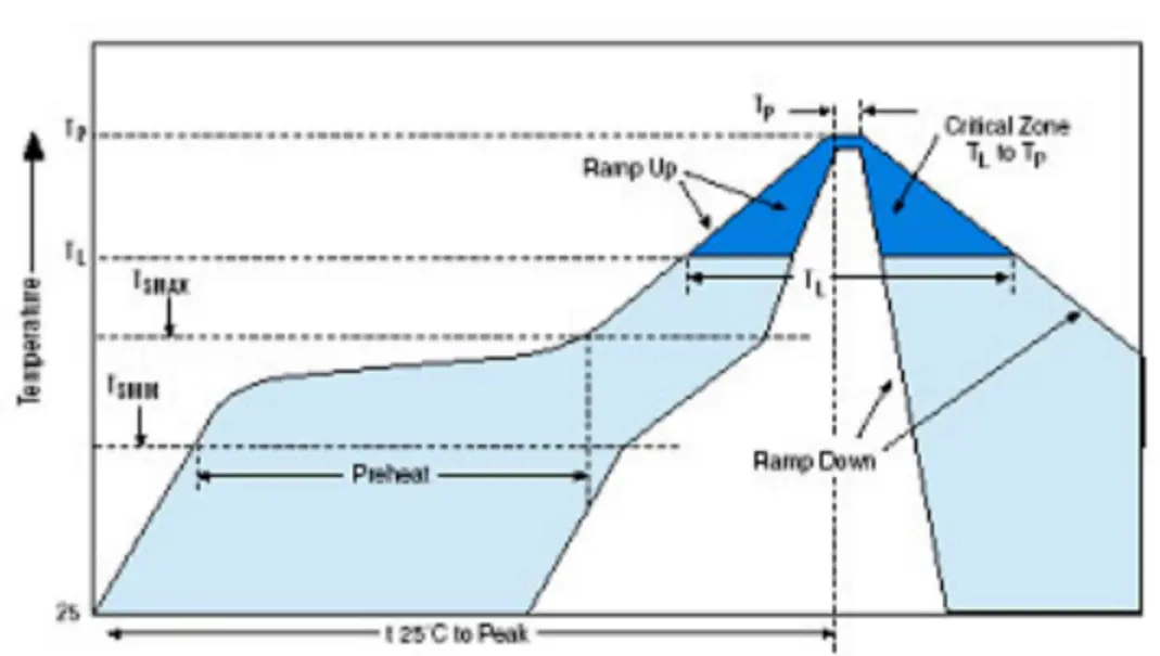
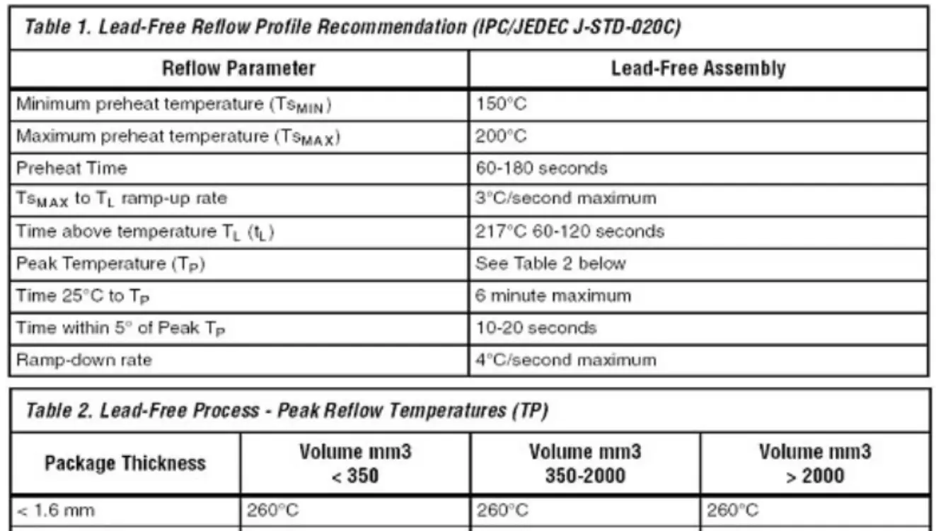
Lead-free technology often requires higher soldering temperatures and longer durations. In previous articles on solder alloys, I explained that the alternatives to the widely promoted Sn37Pb alloy all have higher melting points. For the most favored SAC alloys, the melting point is around 217°C (varying slightly based on composition), and NEMI (National Electronics Manufacturing Initiative) recommends a soldering temperature of no less than 235°C. Many in the industry have found that 240°C to 250°C is ideal, which is about 20°C to 30°C higher than traditional leaded technology. Whether traditional component materials can withstand this higher thermal energy must be evaluated and confirmed. The impact of high temperatures is mainly in four areas. Firstly, whether the component packaging can withstand high temperatures. Secondly, whether higher temperatures exacerbate the impact of moisture absorption on component packaging compared to leaded technology. The third consideration is whether the terminal material and plating thickness can prevent excessive oxidation during high-temperature processing, leading to poor solderability. Finally, at high temperatures, the degree of curvature between the component and the PCB is relatively large, causing poor coplanarity, which can lead to issues such as false soldering and open circuits. To ensure that the components provided by suppliers can meet thermal resistance requirements, IPC/JEDEC has introduced a standard recommendation, J-STD-020C (Figure 1, Tables 1 and 2). It is recommended that all lead-free components must meet this standard. The thermal resistance of all lead-free components should be measured according to the standards suggested. Recognizing the difference in thermal capacities among different packages, Table 2 allows components with higher thermal capacities to withstand lower temperatures. However, this approach is not accepted by all users due to its complexity in management. Users prefer a unified 260°C indicator, but this poses higher requirements for suppliers and is not recognized by all. Clear communication or actual testing and certification must be conducted during procurement if necessary.
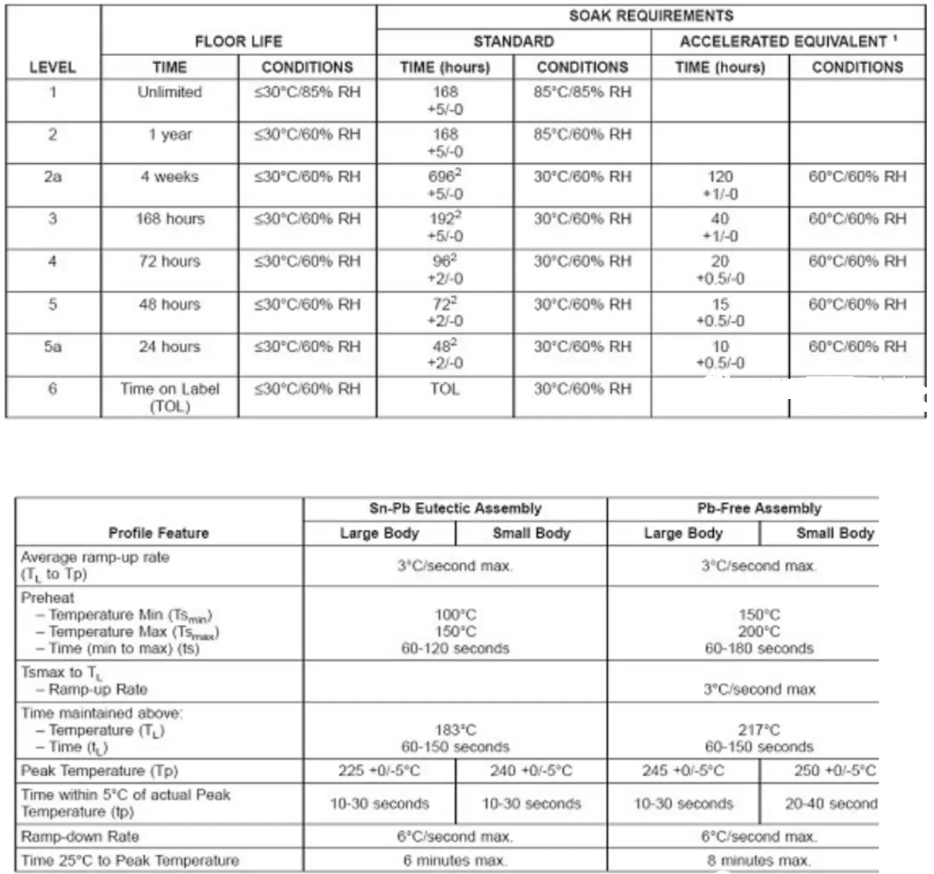
The second consideration is the issue of moisture absorption by components. Generally, plastic-packaged semiconductors and integrated circuits are affected. Due to the increased thermal energy of lead-free soldering, if components absorb moisture, the damage caused by heating will be greater. Industry tests and usage experiences have found that some components are indeed more prone to packaging cracks and "popcorn effects" under lead-free soldering temperature profiles. Since the ratio of vapor to temperature is not linear, under lead-free high-temperature soldering, although the temperature is increased by about 10% to 20% compared to leaded soldering, the measured increase in vapor pressure is as high as 63% to 86%. Imagine the increase in destructive force. Based on tests and experience, the industry mostly believes that the impact of lead-free technology requires increasing the original moisture sensitivity level or sensitivity of components by 1 to 2 levels. The classification of levels can refer to IPC/JEDEC standards (Table 3). IPC/JEDEC also provides methods for certifying component moisture resistance levels, and Tables 3 and 4 show some test parameters and pre-test handling conditions. Problems caused by moisture absorption and high-temperature heating commonly include popcorn effects, package cracks, and internal delamination. Depending on the location and severity, not all issues can be detected by visual inspection. AOI (Automated Optical Inspection) is not suitable for handling this type of inspection, and automated AXI (Automated X-ray Inspection) can detect some issues (but not 100%), but its speed and cost are not suitable for production conditions. Therefore, avoiding such issues must start with component certification before procurement. The above IPC/JEDEC standards can serve as a reference. Users who need more accuracy must negotiate with suppliers to reach mutually agreed results in terms of methods and costs. Another point to note is that although suppliers generally offer baking components before assembly, in lead-free technology, better procurement processes and inventory conditions should be implemented to avoid the need for baking. Baking not only increases work and costs but also increases quality control difficulties for lead-free technology, which already has poor wettability and is prone to porosity issues.
As for the third consideration, regarding whether component terminal plating can withstand higher soldering thermal energy while maintaining good solderability, there is currently no unified standard. Only suppliers or some users involved in this work have empirical data. Due to many sub-factors involved, including materials, types and parameters of plating processes, thickness, inventory conditions and duration, soldering times and parameter settings, etc., it is not easy to formulate and agree on such standards. Therefore, users should ideally have their own research and certification capabilities or sufficient communication with suppliers in this regard. It is important to emphasize that when evaluating supplier reports, the material combinations must be carefully assessed. As I mentioned before, there are many types of lead-free materials, and different combinations often exhibit different performances that cannot be predicted.
The issue of poor coplanarity, although there are some international standards and recommendations in leaded technology, has not been well resolved and controlled in practice. Nowadays, lead-free technology may bring even more severe curvature issues, further exacerbating the problem. Especially for components that originally had difficulty controlling coplanarity, such as connectors and BGAs. The selection of component terminals and packaging materials, DFM specifications (solder pads and stencils), heating settings, etc., all become tasks that must be done meticulously. In lead-free technology, the use of trays, clamping plates, and fixing strips during soldering will be more frequent than in the leaded era.