 PCB
PCB FPC
FPC Rigid-Flex
 FR-4
FR-4 HDI PCB
 Rogers High-Frequency Board
 PTFE Teflon High-Frequency Board
 Aluminum
 Copper Core
 PCB Assembly
 LED light PCBA
 Memory PCBA
 Power Supply PCBA
 New Energey PCBA
 Communication PCBA
 Industrial Control PCBA
 Medical Equipment PCBA
 Testing Service
 PCBA Testing Service
 Certification Application
 RoHS Certification Application
 REACH Certification Application
 CE Certification Application
 FCC Certification Application
 CQC Certification Application
 UL Certification Application
 Transformers, Inductors
 High Frequency Transformers
 Low Frequency Transformers
 High Power Transformers
 Conversion Transformers
 Sealed Transformers
 Ring Transformers
 Inductors
 Wires,Cables Customized
 Network Cables
 Power Cords
 Antenna Cables
 Coaxial Cables
 Net Position Indicator
 Solar AIS net position indicator
 Capacitors
 Connectors
 Diodes
 Embedded Processors & Controllers
 Digital Signal Processors (DSP/DSC)
 Microcontrollers (MCU/MPU/SOC)
 Programmable Logic Device(CPLD/FPGA)
 Communication Modules/IoT
 Resistors
 Through Hole Resistors
 Resistor Networks, Arrays
 Potentiometers,Variable Resistors
 Aluminum Case,Porcelain Tube Resistance
 Current Sense Resistors,Shunt Resistors
 Switches
 Transistors
 Power Modules
 Isolated Power Modules
 AC-DC Power Modules
 DC-AC Module(Inverter)
 RF and Wireless
Part Two: Detailed Analysis of Lead-Free Materials and Processes for Device Solder Terminals
Part Two: Detailed Analysis of Lead-Free Materials and Processes for DevICe Solder Terminals
In electronic device manufacturing, lead-free solder terminals represent a significant trend. The use of lead in devices extends beyond just leads or solder terminals, encompassing internal processes such as chip assembly. However, here, we primarily discuss the second-level assembly technology that directly affects suRFace mount technology (SMT) users, namely the exposed solder terminals and lead portions of devices.
Device suppliers adopt two primary approaches when addressing lead-free solder terminals. One is tin (Sn)-based alloys, such as pure tin (Sn), tin-copper (SnCu), tin-bismuth (SnBi), and others. The other is tin-free alloys, such as nickel-gold (Ni/Au), palladium-nickel (PdNi), palladium (Pd), and more.
Numerous technically feasible materials have been adopted to varying degrees, including 100% Sn, SnCu, Ni/Au, AgPd, SnAg, SnBi, Ni/Pd, Pd, Ag, SnZn, Ni/Pd/Au, Au, AgPt, SnIn, and SAC. However, not all materials are equally popular. From a supply perspective, there are notable preferences differences between Western industries and Japan.
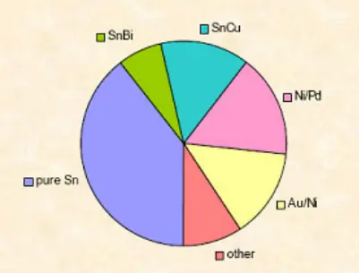
Western suppliers tend to favor 100% Sn (mostly matte tin), while Japan prefers SnBi alloys. Approximately 80% of Western suppliers offer 100% Sn as the primary plating material, while about 86% of Japanese suppliers choose SnBi. Additionally, other popular solder terminal plating materials, in order of popularity, include SnCu, Ni/Pd, Ni/Pd/Au, Ni/Au, SnAg, and SAC.
A large-scale survey of Western users in 2002 revealed these trends. In terms of performance, 100% Sn is closest to traditional tin-lead (SnPb) alloys and has a relatively low cost among lead-free materials, making it popular in the West. However, its main issues include potential risks of whisker formation and rapid intermetallic compound (IMC) growth. Despite significant experience in dealing with these issues, uncertainties remain due to incomplete understanding of the underlying mechanisms.
SAC, SnBi, and Ni/Pd/Au also perform well, but the latter is expensive and scarce due to its palladium and gold content. SnBi is not accepted in the West due to its high lead contamination risk. Ni/Au is slightly inferior to Ni/Pd/Au in wettability but has more practical usage experience. However, its cost is a factor that many customers are unwilling to accept.
SAC alloys are widely adopted (with various compositions) on spherical solder terminal devices such as BGA and CSP. Over 70% of global suppliers choose SAC as the solder terminal material. This is because packages using such solder terminal designs are often difficult to process, so choosing a material identical or very close to the solder reduces process variability. However, it's worth noting that not all users adopt SAC alloy solders, and the same solder may also cause certain process quality issues (such as porosity).
Regarding the characteristics of various popular platings:
100% Sn: Pure tin offers numerous advantages. Its wettability is better among lead-free materials, and its processability is close to SnPb alloys. The reliability of solder joints may even surpass SnPb alloys. Pure tin has no lead contamination issues, and the plating process is stable with no need for alloy composition control. Tin is abundant and relatively low in cost (actually quite close to SnPb in cost). However, pure tin platings also have quality issues such as whiskers, tin pest, and rapid IMC growth. Although the industry largely believes that matte tin can control whisker issues, the underlying mechanisms and control methods are not yet fully understood.
SnBi: This is the most popular material in the Japanese industry. It has good welding processability, extensive practical usage and production experience, and long solder joint lifespans (comparable or slightly higher than SnPb alloys). However, SnBi poses a high lead contamination risk (due to unstable quality), requires strict control of the plating process (thus increasing plating costs), and is difficult to recycle (with high costs to comply with WEEE requirements). Additionally, in wave soldering, bismuth can contaminate the tin bath, increasing the risk of pad or joint peel-off failures. Due to issues with low-melting-point IMCs (posing risks in high-temperature applications), this plating is not accepted by the automotive industry.
SnCu: Commonly used is the Sn0.7Cu alloy, primarily chosen for its low cost (about 20% higher than SnPb) and compatibility with wave soldering alloys. However, since Sn content is high, pure tin's issues and concerns also exist in this material, including whiskers, tin pest, and IMC growth. The Cu composition is sensitive to melting point temperature, so strict control of Cu composition is required during processing to avoid causing unstable process quality.
Ni/Pd and Ni/Pd/Au: These materials have a long history of practical usage and manufacturing experience (since 1989), long shelf lives (up to 8 years in test reports), good wettability and tensile strength (superior to SnPb alloys). However, palladium is naturally scarce, making it costly and unsuitable for use on 42-alloy leads (due to corrosion issues). Additionally, cracks can easily appear at bends after lead forming (although new manufacturing processes are reported to avoid this issue). The Ni layer effectively prevents Cu infiltration into Sn, thus preventing porosity issues in solder joints caused by IMCs and metal migration, which can affect joint lifespan.
Ni/Au: Ni/Au is also one of the materials with extensive usage experience, boasting good shelf lives and wettability. However, its reliability varies greatly, with the key lying in the control of plating thickness. Too thin plating reduces shelf life, while too thick plating affects joint reliability. Additionally, the high cost of Ni/Au technology is a factor hindering its widespread use.
SnAg: The Sn3.5Ag alloy is commonly used. This material has long practical experience, widespread availability, and good reliability. However, the Ag composition significantly affects the melting point temperature, and strict control of alloy composition is required during the plating process. Furthermore, the plating process is complex and not easy to handle environmentally. SnAg's wettability is inferior to SnPb and among the poorer options among the common lead-free platings introduced here. Therefore, appearance inspection standards need to be differentiated.
SAC: This material is widely used on BGA solder terminals and seems to have become the standard. Since BGA package designs are challenging in terms of welding processes, adopting a material with performance closest to the solder alloy is advantageous. Currently, most research institutions, international standards organizations, suppliers, and users favor SAC as the mainstream alloy for future reflow soldering. However, using SAC on BGAs is not without issues. For example, its melting point is the same as the solder paste alloy, raising requirements for reflow temperature profiles and solder paste formulations. Additionally, during the technology transition period, if BGA suppliers have switched to SAC materials while users have not yet entered the lead-free era (still using SnPb solder paste), SAC solder terminals may have difficulty forming good solder joints under traditional SnPb welding temperatures.
Part One: Detailed Analysis of Lead-Free Materials and Processes for Device Solder Terminals