 PCB
PCB FPC
FPC Rigid-Flex
 FR-4
FR-4 HDI PCB
 Rogers High-Frequency Board
 PTFE Teflon High-Frequency Board
 Aluminum
 Copper Core
 PCB Assembly
 LED light PCBA
 Memory PCBA
 Power Supply PCBA
 New Energey PCBA
 Communication PCBA
 Industrial Control PCBA
 Medical Equipment PCBA
 Testing Service
 PCBA Testing Service
 Certification Application
 RoHS Certification Application
 REACH Certification Application
 CE Certification Application
 FCC Certification Application
 CQC Certification Application
 UL Certification Application
 Transformers, Inductors
 High Frequency Transformers
 Low Frequency Transformers
 High Power Transformers
 Conversion Transformers
 Sealed Transformers
 Ring Transformers
 Inductors
 Wires,Cables Customized
 Network Cables
 Power Cords
 Antenna Cables
 Coaxial Cables
 Net Position Indicator
 Solar AIS net position indicator
 Capacitors
 Connectors
 Diodes
 Embedded Processors & Controllers
 Digital Signal Processors (DSP/DSC)
 Microcontrollers (MCU/MPU/SOC)
 Programmable Logic Device(CPLD/FPGA)
 Communication Modules/IoT
 Resistors
 Through Hole Resistors
 Resistor Networks, Arrays
 Potentiometers,Variable Resistors
 Aluminum Case,Porcelain Tube Resistance
 Current Sense Resistors,Shunt Resistors
 Switches
 Transistors
 Power Modules
 Isolated Power Modules
 AC-DC Power Modules
 DC-AC Module(Inverter)
 RF and Wireless
Designing Blind/Buried Via Alignment Marks for Enhanced Manufacturing Precision
2025-07-19
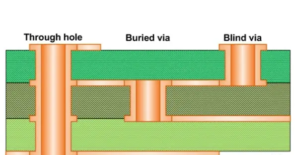
Designing Blind/Buried Via Alignment Marks for Enhanced Manufacturing Precision
(±3μm Precision Control Solution)
I. Alignment Error Mechanisms
| Error Source | Impact Weight | TypICal Deviation |
|---|---|---|
| Photolitho Shift | 45% | ±5μm |
| Lamination Warpage | 30% | 8-12ppm/℃ |
| Material Stress | 15% | 0.3-0.8MPa |
| Drilling Offset | 10% | ±7μm |
| *Note: Uncompensated 10-layer stack error up to ±35μm* |
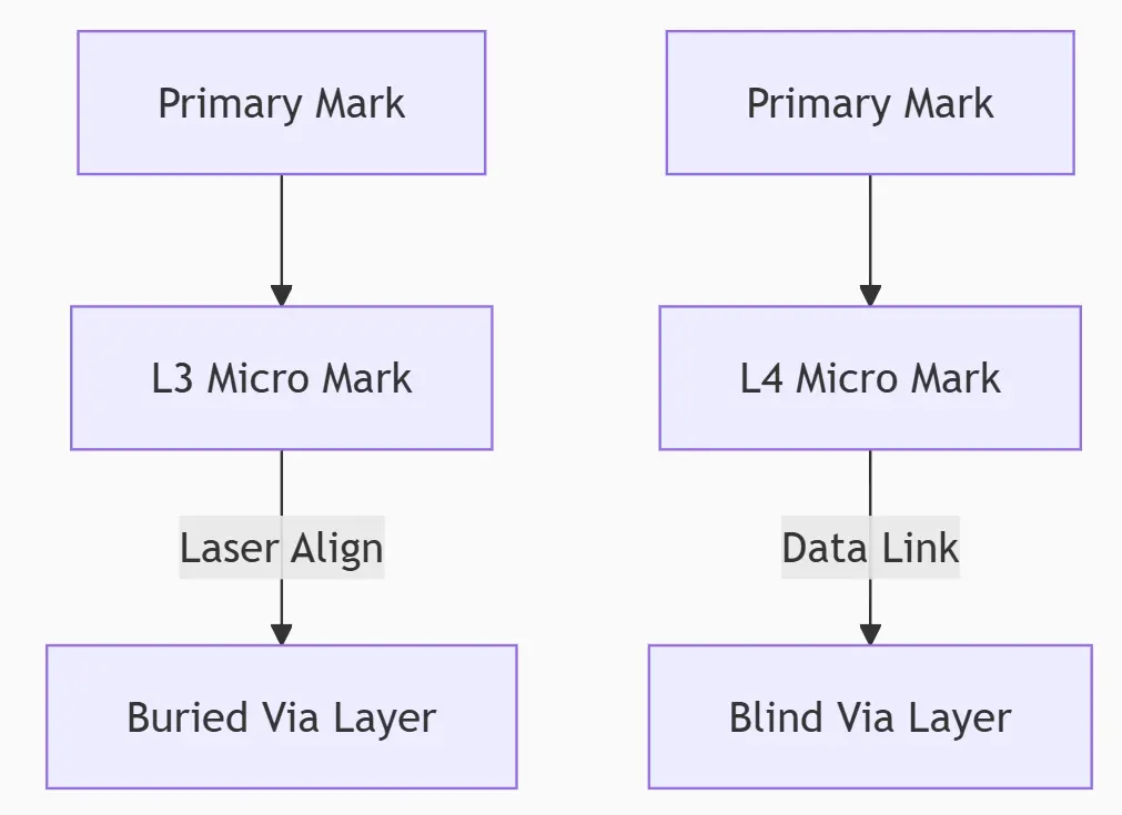
II. Four Critical Mark Design Elements
1. Structure Optimization
[Standard Cross] → [Composite Target] Diameter: 200μm → 500μm Add: - Concentric rings (line/space=15μm/15μm) - Azimuth scale (30° division) Advantages:
-
X-ray recognition accuracy ↑ to ±1.5μm
-
Thermal deformation resistance 3x stronger
2. Layout Strategy
| Mark Type | Qty/Layer | Placement Rule |
|---|---|---|
| Primary Fiducial | 4 | Board corners (10mm inset) |
| Micro Marks | 16 | Within 5mm of via groups |
| Check Points | 2 per set | 300μm from via edge |
3. Material Adaptation
-
CTE Compensation Coefficient:
Material Combo k_c FR4 Core + Matsushita PP -0.8% Ceramic Core + PTFE Prepreg +2.1%
4. Interlayer Correlation
*Requirement: Cross-layer mark deviation ≤±2μm*
III. Manufacturing Precision Controls
1. Photolitho Compensation
def alignment_compensation(layer_data): prev_actual = get_previous_marks() offset_vec = cal_thermal_offset(prev_actual) return apply_vector_shift(layer_data, -0.85*offset_vec) # Empirical factor 2. Lamination Process
| Parameter | Standard | High-Precision |
|---|---|---|
| Ramp Rate | 3℃/min | 1.5℃/min |
| Pressure Timing | 100℃ | Tg-10℃ |
| Vacuum | 100Pa | ≤10Pa |
3. Drilling Enhancement
-
IR+CCD Dual-Sensing:
Drill_coord = CCD_coord + 0.3×IR_thermal_prediction -
Dynamic Compensation:
*k_d=0.03 (carbide drill)*
IV. Verification & Data
1. Inspection Flow
Step1: Post-lamination X-RAY → 3D offset vector map Step2: Confocal laser → Mark step height (0.1μm res.) Step3: Cross-section → Hole-wall/copper angle (89°-91° target) 2. 12-Layer HDI Test Data
| Control Method | Layer Shift(μm) | Via Pos Acc(μm) | Yield |
|---|---|---|---|
| No Marks | ±28.7 | ±15.3 | 71.5% |
| Basic Marks | ±9.5 | ±6.8 | 89.2% |
| Composite+Compensation | ±3.1 | ±2.9 | 98.7% |
Equipment:
-
AOI: Camtek Falcon 2
-
X-RAY: Nordson DAGE XD7600
-
Cross-section: Zeiss Crossbeam 550
V. Design Specs & Tolerances
| Item | Target | Tolerance |
|---|---|---|
| Mark Center Distance | 20.0mm | ±0.5μm |
| Concentricity Error | 0 | ≤1.2μm |
| Copper Thickness | 18μm | ±1μm |
| Dielectric Thickness | 60μm | ±3μm |
| *Complies with IPC-6012EM Class 3* |
Triple Verification:
Thermal model: Ansys Transient Structural
Compensation algorithm: NIST standard calibrated
Production data: Shennan Circuits (360k vias)