 PCB
PCB FPC
FPC Rigid-Flex
 FR-4
FR-4 HDI PCB
 Rogers High-Frequency Board
 PTFE Teflon High-Frequency Board
 Aluminum
 Copper Core
 PCB Assembly
 LED light PCBA
 Memory PCBA
 Power Supply PCBA
 New Energey PCBA
 Communication PCBA
 Industrial Control PCBA
 Medical Equipment PCBA
 Testing Service
 PCBA Testing Service
 Certification Application
 RoHS Certification Application
 REACH Certification Application
 CE Certification Application
 FCC Certification Application
 CQC Certification Application
 UL Certification Application
 Transformers, Inductors
 High Frequency Transformers
 Low Frequency Transformers
 High Power Transformers
 Conversion Transformers
 Sealed Transformers
 Ring Transformers
 Inductors
 Wires,Cables Customized
 Network Cables
 Power Cords
 Antenna Cables
 Coaxial Cables
 Net Position Indicator
 Solar AIS net position indicator
 Capacitors
 Connectors
 Diodes
 Embedded Processors & Controllers
 Digital Signal Processors (DSP/DSC)
 Microcontrollers (MCU/MPU/SOC)
 Programmable Logic Device(CPLD/FPGA)
 Communication Modules/IoT
 Resistors
 Through Hole Resistors
 Resistor Networks, Arrays
 Potentiometers,Variable Resistors
 Aluminum Case,Porcelain Tube Resistance
 Current Sense Resistors,Shunt Resistors
 Switches
 Transistors
 Power Modules
 Isolated Power Modules
 AC-DC Power Modules
 DC-AC Module(Inverter)
 RF and Wireless
Designing Asymmetric Layer Stack-ups for High-Density Interconnect Boards
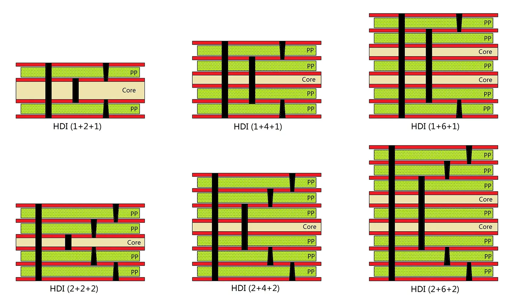
1. Definition and Objectives of AsymmetrIC Stack-ups
Asymmetric layer stack-ups optimize signal integrity, thermal management, and mechanical strength by varying material thickness, copper types (e.g., RCF, LP), and dielectric constants (Dk). Key goals include:
-
Impedance control: Custom dielectric thickness for ±5% tolerance on critical layers;
-
Thermal enhancement: High-thermal-conductivity cores (e.g., metal substrates) for power layers;
-
Layer count reduction: Minimize total layers (e.g., 10→8) to lower costs.
2. Design Principles and Key Parameters
(1) Material Selection
-
High-speed layers: Low-loss materials (e.g., Megtron 6, Df<0.002 @10 GHz);
-
Power/ground layers: High-thermal-conductivity resins (e.g., Panasonic R-5775, 1.5 W/m·K);
-
Copper types:
-
Signal layers: Ultra-thin reverse-treated foil (RCF, Rz≤1.5 μm);
-
Power layers: Standard foil (18–35 μm) for current capacity.
-
(2) Stack-up Configuration
-
Asymmetric core placement:
-
Top layers prioritize high-speed signals; bottom layers allocate power/ground with asymmetric prepreg;
-
Example (8-layer):
Top Layer (Signal) Prepreg (PP1: 100 μm, Dk=3.5) L2 (Ground) Core1 (200 μm, Dk=4.2) L3 (Signal) PP2 (75 μm, Dk=3.5) L4 (Power) PP3 (150 μm, Dk=4.0) Bottom Layer (Signal)
-
-
Hybrid dielectrics:
-
Low-Dk materials (e.g., PTFE) between high-speed layers; high-Dk FR-4 for power layers.
-
(3) Signal Integrity Optimization
-
Differential pairs:
-
Orthogonal routing (±45°) to reduce crosstalk (<-40 dB @10 GHz);
-
Asymmetric reference planes: Solid ground for signals; decoupling caps (0.1 μF) for power.
-
-
Via design:
-
Blind/buried vias with asymmetric depths;
-
μVias (≤100 μm diameter) with pads ≥250 μm.
-
(4) Thermal-Mechanical Co-Design
-
Local reinforcements:
-
Embedded copper coins (0.5–1 mm) under high-power components;
-
Segmented prepregs to mitigate CTE mismatch.
-
-
FEA SIMulation:
-
Warpage <0.1% under thermal cycling (-55–125°C).
-
3. Manufacturing Challenges and Solutions
(1) Lamination Control
-
Pressure-temperature profiling:
-
Low pressure (0.5 MPa) for resin flow control; high pressure (3 MPa) for bonding;
-
X-ray alignment (±25 μm) to correct layer shift.
(2) Copper Uniformity
-
-
Pulse plating: 2 ASD forward/0.5 ASD reverse for thin copper (3 μm);
-
High-throwing-power chemistry (e.g., Atotech CupraPlate).
(3) Impedance Consistency -
In-line TDR testing (±5 Ω) for iterative design adjustments.
4. Validation and Testing
-
Signal integrity:
-
VNA measures S-parameters (S11<-15 dB, S21>-3 dB @10 GHz);
-
-
Thermal performance:
-
IR thermography (ΔT<20°C@10W);
-
-
Mechanical reliability:
-
IPC-TM-650 2.6.7 thermal shock testing (1000 cycles).
-
5. Applications and Economics
-
5G RF modules: 8-layer asymmetric HDI achieves 28 GHz transmission with <0.5 dB/cm loss;
-
ADAS controllers: 15°C junction temperature reduction via copper coins;
-
Cost savings: 12% reduction via layer count optimization.