To simplify and improve the printed circuit soldering process, the Pin-in-Paste technology has been specifically developed. It replaces the original Dipping process for through-hole connectors with the SMT process of printing solder paste and then passing through a reflow oven. All through-hole components must be designed on the same side to avoid inte
RFering with solder paste printing.
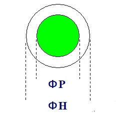
(1) Principle of the Ratio (PH) between Component Lead Diameter and Through-Hole Diameter:
- A PH value of 0.6 - 0.8 is preferred; a PH value of 0.4 - 0.5 is acceptable; a PH value less than 0.4 is poor.
PH=Maximum Cross-Sectional Diameter of Component Lead/Maximum Cross-Sectional Diameter of Through-Hole|=φP/φH
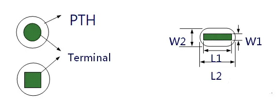
(2) Classification of Component Lead Cross-Section Shapes: Circular, Square, or Rectangular
- Circular through-holes are suitable for circular and square component leads, and the dimensions must meet the requirement: 0.36 ≤ A(P)÷A(H) ≤ 0.5.
- Oval through-holes are suitable for rectangular component leads, and the dimensions must meet the requirement: L2:W2 ≥ 1.5:1.
A(P) = Maximum Cross-Sectional Area of Component Lead; A(H) = Maximum Cross-Sectional Area of Through-Hole
L2 ≈ L1 + 0.4 mm; W2 ≈ W1 + 0.4 mm
(3) Solder Paste Printing Restricted Area: The area of the component text box is the solder paste printing restricted area.
- There should be no test points within the restricted area.
- If there are via holes within the restricted area, they must be covered with green paint.
- There should be no exposed copper foil within the restricted area (it must be covered with green paint).
(4) If the annular pad of any PTH hole is connected to the adjacent
Connector pad, add at least 20 mils wide solder mask to separate them.
(5) To be suitable for the Pin in Paste process, a distance of 2.5 mm needs to be reserved between the through-hole and the pad.
(1) Board Lock / Kink Part:
(i) The layout should be designed with board lock / kink, and it is still mainly oval.
(ii) The dimensions of the oval should meet the ratio: L:W > 1.5:1.
(iii) The size of the oval hole should ensure that the force required to insert the component into the PCB is no more than 2.5 kg. The inserted components on the PCB should not be tilted, toppled, or prone to loosening.
(2) Boss / Guide Pin Part:
(i) The layout should be designed with boss / guide pin.
(ii) The hole diameter size should ensure that the force required to insert the component into the PCB is no more than 2.5 kg.
 PCB
PCB FPC
FPC Rigid-Flex
 FR-4
FR-4 HDI PCB
 Rogers High-Frequency Board
 PTFE Teflon High-Frequency Board
 Aluminum
 Copper Core
 PCB Assembly
 LED light PCBA
 Memory PCBA
 Power Supply PCBA
 New Energey PCBA
 Communication PCBA
 Industrial Control PCBA
 Medical Equipment PCBA
 Testing Service
 PCBA Testing Service
 Certification Application
 RoHS Certification Application
 REACH Certification Application
 CE Certification Application
 FCC Certification Application
 CQC Certification Application
 UL Certification Application
 Transformers, Inductors
 High Frequency Transformers
 Low Frequency Transformers
 High Power Transformers
 Conversion Transformers
 Sealed Transformers
 Ring Transformers
 Inductors
 Wires,Cables Customized
 Network Cables
 Power Cords
 Antenna Cables
 Coaxial Cables
 Net Position Indicator
 Solar AIS net position indicator
 Capacitors
 Connectors
 Diodes
 Embedded Processors & Controllers
 Digital Signal Processors (DSP/DSC)
 Microcontrollers (MCU/MPU/SOC)
 Programmable Logic Device(CPLD/FPGA)
 Communication Modules/IoT
 Resistors
 Through Hole Resistors
 Resistor Networks, Arrays
 Potentiometers,Variable Resistors
 Aluminum Case,Porcelain Tube Resistance
 Current Sense Resistors,Shunt Resistors
 Switches
 Transistors
 Power Modules
 Isolated Power Modules
 AC-DC Power Modules
 DC-AC Module(Inverter)
 RF and Wireless