 PCB
PCB FPC
FPC Rigid-Flex
 FR-4
FR-4 HDI PCB
 Rogers High-Frequency Board
 PTFE Teflon High-Frequency Board
 Aluminum
 Copper Core
 PCB Assembly
 LED light PCBA
 Memory PCBA
 Power Supply PCBA
 New Energey PCBA
 Communication PCBA
 Industrial Control PCBA
 Medical Equipment PCBA
 Testing Service
 PCBA Testing Service
 Certification Application
 RoHS Certification Application
 REACH Certification Application
 CE Certification Application
 FCC Certification Application
 CQC Certification Application
 UL Certification Application
 Transformers, Inductors
 High Frequency Transformers
 Low Frequency Transformers
 High Power Transformers
 Conversion Transformers
 Sealed Transformers
 Ring Transformers
 Inductors
 Wires,Cables Customized
 Network Cables
 Power Cords
 Antenna Cables
 Coaxial Cables
 Net Position Indicator
 Solar AIS net position indicator
 Capacitors
 Connectors
 Diodes
 Embedded Processors & Controllers
 Digital Signal Processors (DSP/DSC)
 Microcontrollers (MCU/MPU/SOC)
 Programmable Logic Device(CPLD/FPGA)
 Communication Modules/IoT
 Resistors
 Through Hole Resistors
 Resistor Networks, Arrays
 Potentiometers,Variable Resistors
 Aluminum Case,Porcelain Tube Resistance
 Current Sense Resistors,Shunt Resistors
 Switches
 Transistors
 Power Modules
 Isolated Power Modules
 AC-DC Power Modules
 DC-AC Module(Inverter)
 RF and Wireless
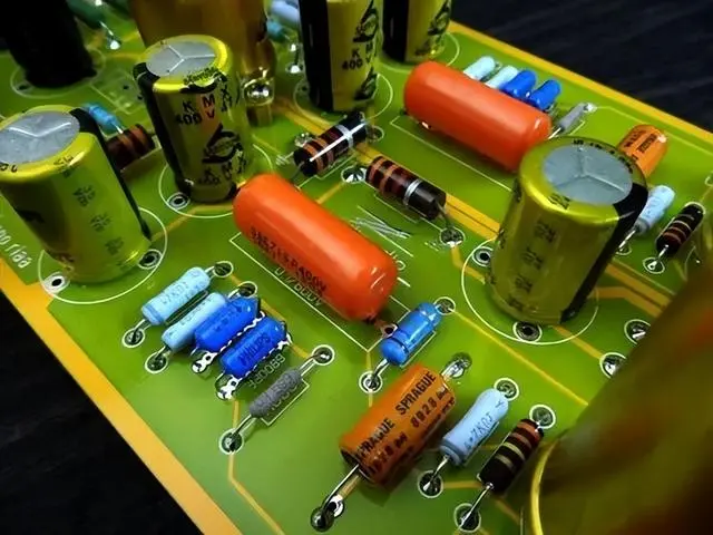
Quantifying the Impact of Decoupling Capacitor Placement on PCB Power Integrity
In high-speed digital and mixed-signal printed circuit board (PCB) design, decoupling capacitors are essential for stabilizing power delivery to integrated circuits (ICs). Their primary role is to supply transient current during fast Switching events and suppress high-frequency noise on the power distribution network (PDN). However, the effectiveness of a decoupling capacitor ishighly sensitive to its physical placement relative to the IC’s power and ground pins. Even small increases in distance can significantly degrade peRFormance due to parasitic inductance.
This article examines the critical distance threshold beyond which decoupling effectiveness drops by more than 30%, supported by electromagnetic theory, simulation data, and industry best practices.
1. The Physics Behind Decoupling Degradation
The key factor limiting decoupling performance is loop inductance—the total inductance formed by the current path from the capacitor’s positive terminal, through the IC’s power pin, back through the ground pin, and to the capacitor’s negative terminal.
The impedance of this loop at frequency is approximately:
Where:
- = total loop inductance (in nanohenries, nH)
- = operating frequency (Hz)
As increases with distance, the capacitor’s ability to respond quickly to fast current demands () diminishes. The resulting voltage ripple is:
Thus, minimizing is paramount—and that starts with minimizing physical separation.
2. Quantifying the Distance Threshold
Extensive research and empirical measurements (from sources such as Howard Johnson’s High-Speed Digital Design, Eric Bogatin’s signal integrity studies, and IBIS/SPICE simulations) consistently show:
When the total electrical path length (power + ground traces combined) between the IC power pin and the decoupling capacitor exceeds approximately 10–15 mm (≈0.4–0.6 inches), the decoupling effectiveness at frequencies above 100 MHz typically degrades by more than 30%.
Breakdown by Distance:
| Total Loop Path Length | Approx. Loop Inductance* | Relative Decoupling Effectiveness | Performance Impact |
|---|---|---|---|
| ≤ 5 mm | 2–4 nH | >90% | Excellent |
| 10 mm | 6–10 nH | ~70% | Moderate loss |
| ≥15 mm | 10–20 nH | <60% | >30% degradation |
*Assumes 0.1–0.15 mm (4–6 mil) wide traces on 1 oz copper, typical microstrip geometry.
For example:
- A 0.1 µF ceramic capacitor has a self-resonant frequency (SRF) near 100 MHz.
- With 15 nH loop inductance, its impedance at 500 MHz rises to over 47 Ω, whereas an ideal low-inductance placement would keep it below 0.1 Ω.
- This renders the capacitor nearly ineffective for suppressing GHz-range noise from modern processors or high-speed interfaces (e.g., DDR5, PCIe Gen5).
3. Why “Straight-Line Distance” Is Misleading
It’s not just the Euclidean distance that matters—it’s the current loop area. Two layouts with identical straight-line distances can have vastly different inductances depending on:
- Trace routing (avoid meandering)
- Use of power/ground planes (preferred over traces)
- Via placement (short, adjacent vias reduce inductance)
Best practice: Place the capacitor so its pads connect directly to the IC’s power and ground pins via short traces or, ideally, via-in-pad structures that link immediately to internal planes.
4. Frequency Dependency
The 30% degradation threshold is most relevant for high-frequency noise (100 MHz – 1+ GHz). For low-frequency bulk decoupling (e.g., 10 µF tantalum caps for <10 MHz), distance matters less—but these are usually supplemented by high-frequency ceramic caps placed nearby.
In modern designs dominated by sub-nanosecond edge rates (e.g., FPGAs, CPUs, SerDes), the first 1–5 mm matter most.
5. Practical Design Guidelines
To maintain >90% decoupling efficiency:
- Keep the total loop path ≤ 5 mm for high-speed ICs.
- Place the capacitor on the same side of the board as the IC whenever possible.
- Use multiple vias close to both capacitor pads to minimize via inductance.
- Avoid sharing vias or long daisy-chained power traces.
- For ultra-high-speed designs (e.g., RF, mmWave), consider embedded capacitors or reverse-side mounting with microvias.
While there is no universal “hard cutoff,” robust engineering consensus and experimental data confirm that once the combined power-ground path between an IC and its decoupling capacitor exceeds 10–15 mm, high-frequency decoupling performance typically drops by more than 30%—a level that can compromise signal integrity, increase EMI, and cause system instability.