1. Core Requirements of DDR4 Routing
Underlying LogIC for Topology Selection As a high-speed synchronous dynamic random-access memory (DDR4, with a maximum data rate of 3200Mbps and up to 4800Mbps for overclocked versions), the core goals of DDR4 routing are to control signal skew, suppress reflections, and reduce crosstalk, while meeting three key specifications:
1. Timing Synchronization: The signal delay difference (tDQSS, Data Queue Skew) between all memory chips (or DIMM slots) and the controller (CPU/memory controller) must be ≤25ps to avoid data sampling errors;
2. Impedance Matching: The characteristic impedance of the signal path must be stable at 50Ω±10% to minimize signal reflection (reflection coefficient Γ≤0.1);
3. Load Capacity: The topology must support DDR4’s load count specifications (up to 2 slots for UDIMMs, up to 8 slots for RDIMMs) without excessive signal attenuation (insertion loss ≤[email protected]).
The selection between T-Topology and Fly-by Topology essentially involves finding the optimal balance among the above specifications through different signal distribution methods. There is no absolute "superior" topology—only "scenario-specific suitability."
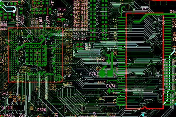
- Structural Principle: The memory controller (signal source) is located at the vertical end of the "T." The main signal line extends and branches at the midpoint (forming the horizontal end of the "T"), with memory loads (chips/DIMM slots) symmetrically distributed on both sides of the branch. The signal path length difference between all loads and the controller is ≤5mm (ideally identical), as shown in Figure 1.
- Core Characteristics:
- Timing Advantage: Consistent path lengths result in minimal delay skew (tDQSS≤10ps), eliminating the need for complex timing compensation and making it suitable for high data rates (3200Mbps and above);
- Impedance Risk: Impedance discontinuities easily occur at branch points (mismatch between the main line and branches). This can be mitigated by "branch length control" (branch length ≤15mm) and "impedance calibration" (branch impedance matches the main line at 50Ω);
- Load Limitation: Supports a maximum of 2–4 loads (e.g., 2 UDIMM slots). Excessive loads increase branch count, exacerbating impedance discontinuities and rAISing signal reflection rates to over 15% (exceeding DDR4’s 10% limit).
- Structural Principle: The controller (signal source) transmits signals along a single main line in a "serial chain"—first reaching the first load, then the second, and so on to the last load. Path lengths from the controller to each load increase sequentially (differences up to 20–50mm), as shown in Figure 2.
- Core Characteristics:
- Load Advantage: No branch points ensure stable impedance (reflection rate ≤8), supporting more loads (up to 8 RDIMM slots) for server-grade multi-memory scenarios;
- Timing Compensation: Large path length differences require "routing length compensation" (extending the main line by 2–3mm for each subsequent load to offset delay) and "dynamic ODT (On-Die Termination) adjustment" (enabling ODT at the last load to absorb reflected signals) to ensure tDQSS≤25ps;
- Rate Limitation: At high data rates (e.g., 4800Mbps), timing compensation becomes challenging, and signal jitter tends to exceed specifications (>10ps). It is more suitable for medium-high speed scenarios (2400–3200Mbps).
DDR4 load count directly determines topology compatibility, making it the "first priority" for selection:
- Loads ≤2 (e.g., consumer electronics: laptops, desktop UDIMMs):
Prioritize T-Topology—Two loads can be symmetrically placed on both sides of the T-branch, with path length differences ≤3mm. Timing synchronization requires no compensation, ensuring optimal signal integrity (reflection rate ≤5%). Forcing Fly-by here adds unnecessary design complexity without leveraging its load capacity advantage. - Loads ≥3 (e.g., servers, workstation RDIMMs):
Mandatorily select Fly-by Topology—Three loads in T-Topology require three branches, where impedance discontinuities cause excessive signal attenuation (insertion loss >4dB), failing DDR4 requirements. Fly-by’s serial structure has no branches; even with 8 loads, impedance remains stable (insertion loss ≤3dB), and reflections are suppressed via ODT.
Note: Per DDR4 specifications, UDIMMs (Unbuffered DIMMs) support a maximum of 2 slots, while RDIMMs (Registered DIMMs) support up to 8 slots. Topology selection must strictly align with this standard.
Signal peRFormance of the two topologies varies significantly across different data rates:
- Rate ≥3600Mbps (overclocked DDR4, high-performance PCs):
Prioritize T-Topology—No branch-induced timing skew limits jitter to ≤8ps, meeting high-bandwidth needs (e.g., 28.8GB/s for dual-channel 3600Mbps). Fly-by’s timing compensation fails at high rates, increasing jitter to >12ps and raising bit error rates (BER >1e-12). - Rate ≤3200Mbps (conventional scenarios: office PCs, entry-level servers):
Both topologies work, but Fly-by is preferred—At medium speeds, Fly-by easily meets tDQSS≤25ps with length compensation (max length difference ≤30mm). Its simple structure (no branches) saves 20–30% of PCB routing space, reducing design costs.
Physical PCB space and layer count affect topology implementation feasibility:
- Fewer PCB layers (4-layer boards, consumer electronics) and compact layouts:
Prioritize Fly-by Topology—A single main line requires no branches, occupying only one signal layer. The main line can be routed along PCB edges to avoid other components (e.g., CPUs, power chips). T-Topology’s branches demand more horizontal space, which may be unavailable on 4-layer boards (risk of signal crosstalk). - More PCB layers (6–8-layer boards, servers) and spacious layouts:
Prioritize T-Topology (if loads ≤2)—Multi-layer boards can allocate a dedicated "memory signal layer," allowing branch routing via vias to avoid crosstalk. Additionally, complete ground planes in multi-layer boards further reduce crosstalk at T-branch points (crosstalk ≤-25dB).
Topology selection must balance design difficulty and mass-production costs:
- Low complexity, low-cost needs (e.g., entry-level desktops):
Choose Fly-by Topology—No branches simplify routing rules (only main line impedance and length compensation need control), resulting in a high DRC (Design Rule Check) pass rate (>95%). No additional impedance calibration components reduce mass-production costs by 5–10% compared to T-Topology. - High reliability, low timing risk (e.g., industrial control, medical devices):
Choose T-Topology (if loads ≤2)—No timing compensation eliminates failures from compensation errors (e.g., memory blue screens due to insufficient Fly-by compensation). The symmetric structure offers high signal redundancy; even minor PCB manufacturing deviations (e.g., ±0.1mm trace width) do not disrupt timing stability.
- Branch Length and Impedance Control:
- Branch length ≤15mm (from main line branch point to load pin), with length differences between two branches ≤2mm;
- Both main line and branches are designed for 50Ω impedance (adjusted via trace width: 0.25mm for 4-layer top/bottom layers, 0.3mm for inner layers). Avoid abrupt width changes at branch points (use "gradual transitions" with width change rates ≤10%/mm).
- Crosstalk Suppression:
- Maintain a spacing of ≥3W (W = memory trace width) between memory signals and other high-speed signals (e.g., PCIe), with a complete ground plane below (no slots or splits);
- Maintain a spacing of ≥2W between adjacent memory signals (e.g., DQS and DQ) to minimize differential pair crosstalk (crosstalk ≤-30dB).
- ODT Configuration:
Enable ODT (50Ω impedance) at all load ends (memory chips/DIMMs) and disable ODT at the controller to absorb reflections at branch points.
- Length Compensation and Timing Calibration:
- Increase main line length sequentially by load order: If the first load is L distance from the controller, the second is L+2mm, and the third is L+4mm (adding 2mm per load) to offset delay differences;
- Align length compensation for critical signals (e.g., clock CLK, data strobe DQS) with data signals (DQ) to ensure tDQSS≤25ps.
- Termination Resistors and Impedance Matching:
- Add a 50Ω series termination resistor (0402 package) at the end of the main line after the last load to work with ODT and suppress far-end reflections;
- Maintain 50Ω impedance throughout the main line, avoiding fluctuations (≤±5%) from trace width changes (e.g., narrowing to bypass components).
- Signal Path Planning:
Route the main line in straight segments to minimize via count (each via introduces 0.5–1ps delay). If vias are necessary, use "impedance-matched vias" (0.3mm drill diameter, 0.8mm anti-pad diameter).
- Selection: T-Topology;
- Reasons: Two loads are symmetrically distributed, with T-Topology timing skew ≤8ps (no compensation needed). Although 4-layer PCBs have limited space, two branches can be routed along PCB edges without occupying core areas. At 3200Mbps, T-Topology offers better signal integrity than Fly-by (4% vs. 7% reflection rate).
- Selection: Fly-by Topology;
- Reasons: Six loads exceed T-Topology’s capacity. 8-layer PCBs can allocate a dedicated signal layer, making main line length compensation (max difference 50mm) feasible. At 2933Mbps, jitter is controlled to ≤9ps after timing compensation, meeting server reliability requirements.
- Selection: Simplified Fly-by (point-to-point topology for single loads);
- Reasons: A single load requires no T-Topology branches, making Fly-by’s single main line simpler. The 6-layer PCB’s complete ground plane limits crosstalk to ≤-35dB, and no complex compensation is needed at 2400Mbps, reducing design costs.
- Root Cause: Overlooking advancements in Fly-by timing compensation;
- Mitigation: At rates ≤3200Mbps, Fly-by meets DDR4 requirements with length compensation + ODT and offers better load capacity. T-Topology is only preferred for rates ≥3600Mbps.
- Root Cause: Ignoring impedance discontinuities at branch points;
- Mitigation: T-Topology supports a maximum of 4 loads with ≤2 branches (i.e., 2 branches at the T’s horizontal end). Exceeding this increases reflection rates, requiring a switch to Fly-by.
- Root Cause: Overlooking the impact of main line impedance fluctuations;
- Mitigation: Fly-by’s main line impedance must remain stable at 50Ω±5%. Vias and trace width changes require calibration; otherwise, signal attenuation increases by 2–3dB.
The selection between T-Topology and Fly-by in DDR4 routing follows the core logic of "loads define topology, rate refines details, layout enables implementation":
- First, "qualify" by load count: ≤2 loads → T-Topology; ≥3 loads → Fly-by;
- Then, "optimize details" by rate: Enhance branch impedance control for T-Topology at high rates (≥3600Mbps); simplify compensation for Fly-by at medium-low rates (≤3200Mbps);
- Finally, "implement" by PCB layout: Choose Fly-by for fewer layers to save space; choose T-Topology for more layers to reduce crosstalk.
The two topologies are not opposites but "optimal solutions" for different DDR4 scenarios. With precise selection and routing optimization, both can meet DDR4’s signal integrity and reliability requirements, maximizing memory performance.
 PCB
PCB FPC
FPC Rigid-Flex
 FR-4
FR-4 HDI PCB
 Rogers High-Frequency Board
 PTFE Teflon High-Frequency Board
 Aluminum
 Copper Core
 PCB Assembly
 LED light PCBA
 Memory PCBA
 Power Supply PCBA
 New Energey PCBA
 Communication PCBA
 Industrial Control PCBA
 Medical Equipment PCBA
 Testing Service
 PCBA Testing Service
 Certification Application
 RoHS Certification Application
 REACH Certification Application
 CE Certification Application
 FCC Certification Application
 CQC Certification Application
 UL Certification Application
 Transformers, Inductors
 High Frequency Transformers
 Low Frequency Transformers
 High Power Transformers
 Conversion Transformers
 Sealed Transformers
 Ring Transformers
 Inductors
 Wires,Cables Customized
 Network Cables
 Power Cords
 Antenna Cables
 Coaxial Cables
 Net Position Indicator
 Solar AIS net position indicator
 Capacitors
 Connectors
 Diodes
 Embedded Processors & Controllers
 Digital Signal Processors (DSP/DSC)
 Microcontrollers (MCU/MPU/SOC)
 Programmable Logic Device(CPLD/FPGA)
 Communication Modules/IoT
 Resistors
 Through Hole Resistors
 Resistor Networks, Arrays
 Potentiometers,Variable Resistors
 Aluminum Case,Porcelain Tube Resistance
 Current Sense Resistors,Shunt Resistors
 Switches
 Transistors
 Power Modules
 Isolated Power Modules
 AC-DC Power Modules
 DC-AC Module(Inverter)
 RF and Wireless