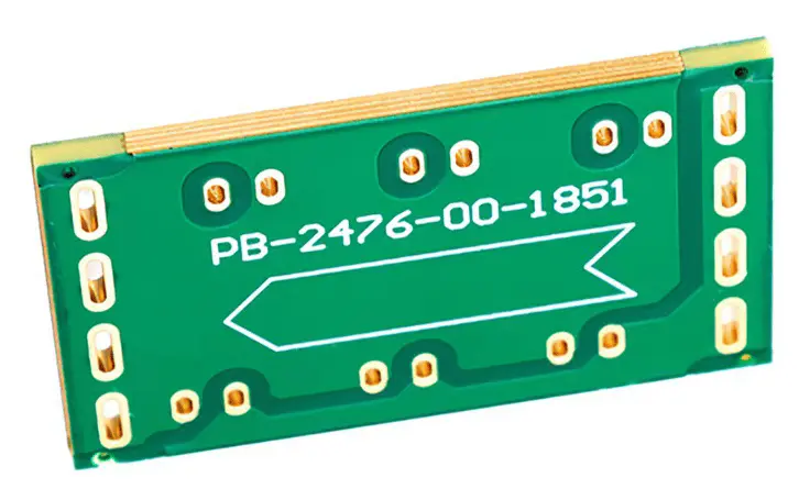
 PCB
PCB FPC
FPC Rigid-Flex
 FR-4
FR-4 HDI PCB
 Rogers High-Frequency Board
 PTFE Teflon High-Frequency Board
 Aluminum
 Copper Core
 PCB Assembly
 LED light PCBA
 Memory PCBA
 Power Supply PCBA
 New Energey PCBA
 Communication PCBA
 Industrial Control PCBA
 Medical Equipment PCBA
 Testing Service
 PCBA Testing Service
 Certification Application
 RoHS Certification Application
 REACH Certification Application
 CE Certification Application
 FCC Certification Application
 CQC Certification Application
 UL Certification Application
 Transformers, Inductors
 High Frequency Transformers
 Low Frequency Transformers
 High Power Transformers
 Conversion Transformers
 Sealed Transformers
 Ring Transformers
 Inductors
 Wires,Cables Customized
 Network Cables
 Power Cords
 Antenna Cables
 Coaxial Cables
 Net Position Indicator
 Solar AIS net position indicator
 Capacitors
 Connectors
 Diodes
 Embedded Processors & Controllers
 Digital Signal Processors (DSP/DSC)
 Microcontrollers (MCU/MPU/SOC)
 Programmable Logic Device(CPLD/FPGA)
 Communication Modules/IoT
 Resistors
 Through Hole Resistors
 Resistor Networks, Arrays
 Potentiometers,Variable Resistors
 Aluminum Case,Porcelain Tube Resistance
 Current Sense Resistors,Shunt Resistors
 Switches
 Transistors
 Power Modules
 Isolated Power Modules
 AC-DC Power Modules
 DC-AC Module(Inverter)
 RF and Wireless
Copper Thickness Selection Criteria for General-Purpose Power PCBs (1–5A Current Rating)
2025-12-11
General-purpose power PCBs, designed to handle current levels ranging from 1A to 5A, are ubiquitous in consumer electronICs, household appliances, and low-power industrial control systems. These boards power devices such as smartphone chargers, LED drivers, small motor controllers, and audio amplifiers, where reliability, cost-effectiveness, and thermal stability are core design priorities. Among the critical design decisions for these power PCBs, copper foil thickness selection stands out as a foundational factor that directly impacts current-carrying capacity, thermal peRFormance, mechanical durability, and manufacturing costs. Common copper thicknesses used in this current range include 1oz (35μm), 1.5oz (52.5μm), and 2oz (70μm), with each option offering distinct trade-offs between performance and cost. This article systematically explores the technical principles, calculation methods, and practical guidelines for selecting the optimal copper thickness for 1–5A power PCBs, drawing on industry standards (IPC-2221), thermal simulation data, and real-world application cases to provide a comprehensive, evidence-based reference for PCB designers and engineers.
1. Fundamental Concepts: Copper Thickness, Current Capacity, and Thermal Performance
To understand copper thickness selection, it is essential to establish the relationship between copper foil properties, current-carrying capability, and heat dissipation—three interconnected parameters that define power PCB performance.
1.1 Definition of Copper Thickness in PCB Design
In PCB manufacturing, copper foil thickness is typically specified in ounces per square foot (oz/ft²), a unit that denotes the mass of copper covering one square foot of the PCB surface. This unit is directly convertible to metric thickness, with industry-standard equivalents as follows:
- 1oz copper foil = 35μm (micrometers) thickness
- 1.5oz copper foil = 52.5μm thickness
- 2oz copper foil = 70μm thickness
For general-purpose power PCBs (1–5A), thicknesses beyond 2oz are rarely used, as they increase material costs, reduce PCB flexibility, and may cause issues with solder mask application and component mounting. Conversely, copper thicknesses below 1oz (e.g., 0.5oz) are insufficient for even 1A continuous current, as they lead to excessive temperature rise and copper trace degradation over time.
1.2 Current-Carrying Capacity: The Core Selection Driver
The primary function of copper traces in power PCBs is to conduct electrical current from the input source to the load while maintaining a safe operating temperature. The current-carrying capacity of a copper trace—defined as the maximum continuous current it can carry without exceeding a specified temperature rise—is determined by four key factors:
- Copper thickness: Thicker copper reduces resistance and allows higher current flow for the same temperature rise.
- Trace width: Wider traces increase the cross-sectional area of the conductor, further lowering resistance and improving heat dissipation.
- Ambient temperature: Higher ambient temperatures reduce the allowable current capacity, as the temperature difference between the trace and the environment is reduced.
- Trace length: Longer traces have higher total resistance, leading to greater power dissipation (P=I²R) and temperature rise.
The relationship between these parameters is quantified by the IPC-2221 standard, which provides empirical formulas and lookup tables for calculating current capacity based on copper thickness, trace width, and temperature rise. For 1–5A power PCBs, the most critical constraint is the maximum allowable temperature rise—typically 10°C to 30°C above ambient temperature (25°C), depending on the application’s reliability requirements.
1.3 Thermal Performance: A Secondary but Critical Consideration
In 1–5A power PCBs, heat generation is primarily caused by resistive losses in copper traces (Joule heating). While the current levels are relatively low compared to high-power industrial PCBs, excessive temperature rise can still cause two key issues:
- Solder joint degradation: Elevated temperatures accelerate solder fatigue, leading to cracked joints and intermittent connections over time.
- Substrate damage: Prolonged exposure to temperatures above the substrate’s glass transition temperature (T₉, typically 120°C for standard FR-4) can cause the PCB to warp or delaminate.
Thicker copper foil improves thermal performance by increasing the trace’s heat-spreading area, allowing heat to dissipate more effectively to the surrounding air and adjacent copper planes. For example, a 2oz copper trace has twice the cross-sectional area of a 1oz trace of the same width, reducing its resistance by 50% and cutting resistive power losses in half for the same current.
2. IPC-2221 Standard: Quantitative Guidelines for Copper Thickness Selection
The IPC-2221 standard is the global benchmark for PCB design, providing engineers with a structured framework to calculate current-carrying capacity and select appropriate copper thicknesses. For general-purpose power PCBs (1–5A), the standard’s guidelines can be simplified into lookup tables and practical formulas that balance accuracy and ease of use.
2.1 IPC-2221 Current-Carrying Capacity Formulas
IPC-2221 specifies two formulas for calculating current capacity: one for internal traces (sandwiched between Pcb Layers, with limited heat dissipation) and one for external traces (exposed to air, with better heat dissipation). For 1–5A power PCBs, external traces are more common, as they facilitate easier heat dissipation and are less prone to overheating.
The formula for external copper traces is: 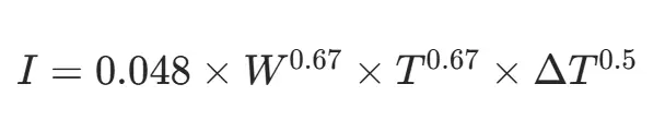
Where:
Where:
- I = Current-carrying capacity (A)
- W = Trace width (mm)
- T = Copper thickness (μm)
- Delta T= Temperature rise above ambient (°C)
Rearranging this formula to solve for copper thickness (T) allows designers to select the minimum thickness required to carry a given current with a specified temperature rise: 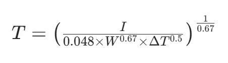
2.2 Current Capacity Comparison for 1oz, 1.5oz, and 2oz Copper
To illustrate the impact of copper thickness on current capacity, Table 1 compares the maximum continuous current that can be carried by external traces of different widths and thicknesses, assuming a temperature rise of 20°C (a common requirement for consumer electronics).
| Trace Width (mm) | 1oz Copper (35μm) – Max Current (A) | 1.5oz Copper (52.5μm) – Max Current (A) | 2oz Copper (70μm) – Max Current (A) |
|---|---|---|---|
| 0.5 | 1.2 | 1.6 | 1.9 |
| 1.0 | 2.0 | 2.7 | 3.2 |
| 1.5 | 2.7 | 3.6 | 4.3 |
| 2.0 | 3.3 | 4.4 | 5.2 |
| 2.5 | 3.9 | 5.2 | 6.2 |
Table 1: IPC-2221 Current Capacity for External Traces (ΔT=20°C, Ambient Temperature=25°C)
Key observations from Table 1:
- For a 1mm wide trace (a common width in compact power PCBs), 1oz copper can carry 2.0A, 1.5oz copper can carry 2.7A, and 2oz copper can carry 3.2A—demonstrating a direct correlation between thickness and current capacity.
- To carry 5A with a 20°C temperature rise, a 2oz copper trace requires a width of 2.0mm, while a 1oz copper trace would need a width of 3.3mm—significantly increasing the PCB’s footprint.
- For low-current applications (1–2A), 1oz copper is sufficient for traces wider than 0.5mm, offering the best balance of cost and performance.
2.3 Adjustments for Internal Traces and High Ambient Temperatures
Internal traces—located between PCB layers—have limited heat dissipation, as they are surrounded by dielectric materials (e.g., FR-4) with low thermal conductivity (0.3–0.5 W/m·K). As a result, their current-carrying capacity is 30–40% lower than that of external traces of the same thickness and width. For example, a 1mm wide 1oz internal trace can only carry 1.2A (vs. 2.0A for an external trace) with a 20°C temperature rise.
High ambient temperatures (e.g., 40°C in enclosed electronic enclosures) also reduce current capacity. For every 10°C increase in ambient temperature, the allowable current capacity decreases by approximately 10%. For a 2oz copper trace designed to carry 5A at 25°C ambient, the maximum current drops to 4.5A at 35°C ambient and 4.0A at 45°C ambient.
3. Key Factors Influencing Copper Thickness Selection for 1–5A Power PCBs
While IPC-2221 provides quantitative guidelines, practical copper thickness selection requires considering additional factors, including PCB layout constraints, cost, mechanical durability, and application-specific requirements.
3.1 PCB Layout and Space Constraints
Compact power PCBs (e.g., smartphone chargers, LED driver modules) often have strict space limitations, requiring designers to minimize trace widths. In such cases, thicker copper foil is the only viable option to meet current-carrying requirements without increasing trace width. For example:
- A 1A LED driver with a maximum trace width of 0.5mm can use 1oz copper, as shown in Table 1.
- A 3A motor controller with a maximum trace width of 1.0mm requires 1.5oz copper, as a 1oz trace of the same width can only carry 2.0A.
- A 5A power supply with a maximum trace width of 2.0mm requires 2oz copper, as a 1.5oz trace of the same width can only carry 4.4A—insufficient for the 5A current rating.
Conversely, PCBs with ample space can use narrower, thicker copper traces or wider, thinner copper traces to achieve the same current capacity. However, wider traces are often preferred for their better heat dissipation and lower resistance.
3.2 Cost Considerations: Balancing Performance and Manufacturing Expenses
Copper foil is one of the most expensive materials in PCB manufacturing, with cost increasing linearly with thickness. For general-purpose power PCBs, the cost premium for thicker copper is as follows:
- 1.5oz copper: 20–30% more expensive than 1oz copper
- 2oz copper: 40–50% more expensive than 1oz copper
For high-volume consumer electronics (e.g., USB chargers produced in millions of units), even a 20% cost increase per PCB can have a significant impact on total production costs. As a result, 1oz copper is the default choice for 1–2A applications, where space constraints are not critical. Thicker copper (1.5oz or 2oz) is only used when space is limited or when higher reliability is required.
3.3 Mechanical Durability and Trace Integrity
Thicker copper foil improves the mechanical durability of PCB traces, making them more resistant to damage from bending, vibration, and thermal cycling. This is particularly important for power PCBs used in portable devices or industrial environments with mechanical stress. For example:
- 2oz copper traces are less likely to crack under thermal cycling than 1oz traces, as their thicker cross-section can better withstand the expansion and contraction of the PCB substrate.
- Thicker copper traces are more resistant to abrasion during assembly and handling, reducing the risk of open circuits caused by trace damage.
For applications requiring long-term reliability (e.g., 10+ years of operation), 1.5oz or 2oz copper is preferred, even for 1–2A current levels, as it minimizes the risk of trace degradation over time.
3.4 Application-Specific Requirements
Different applications impose unique constraints that influence copper thickness selection. The following are common scenarios for 1–5A power PCBs:
- Consumer Electronics (1–2A): USB chargers, Bluetooth speakers, and smart home devices typically use 1oz copper, prioritizing cost and compactness over maximum durability. Temperature rise limits are often relaxed to 30°C to further reduce trace width.
- Industrial Control Systems (2–3A): Motor controllers, sensor interfaces, and relay drivers often use 1.5oz copper, balancing cost and reliability. These systems require operation in harsh environments (wide temperature ranges, vibration), making thicker copper a worthwhile investment.
- Automotive Electronics (3–5A): On-board chargers, lighting controllers, and power distribution modules use 2oz copper, even for 3A current levels. Automotive applications demand strict reliability standards (e.g., IPC-A-610 Class 2), with temperature rise limits of 10°C to prevent damage to adjacent components.
4. Practical Design Guidelines for Copper Thickness Selection
Based on IPC-2221 standards, thermal simulation data, and real-world manufacturing experience, the following step-by-step guidelines provide a actionable framework for selecting copper thickness for 1–5A power PCBs.
4.1 Step 1: Define the PCB’s Current and Temperature Requirements
- Determine the maximum continuous current: Identify the highest current that will flow through each trace in the PCB (e.g., 5A for the input trace, 2A for the output trace).
- Specify the maximum allowable temperature rise: Based on the application, select a temperature rise limit (ΔT) between 10°C and 30°C. For consumer electronics, ΔT=20–30°C is acceptable; for industrial/automotive applications, ΔT=10–20°C is preferred.
- Note the ambient temperature: Measure or estimate the maximum ambient temperature where the PCB will operate (e.g., 25°C for indoor use, 45°C for automotive underhood use).
4.2 Step 2: Calculate Required Copper Thickness Using IPC-2221 Formulas
- Determine the maximum allowable trace width: Based on PCB layout constraints, define the widest trace that can be used for each current path (e.g., 2.0mm for the 5A input trace).
- Use the IPC-2221 formula (Section 2.1) to calculate the minimum copper thickness required to meet the current and temperature rise requirements.
- Adjust for internal traces: If the trace is internal, multiply the calculated current capacity by 0.6–0.7 to account for reduced heat dissipation, then recalculate the required thickness.
4.3 Step 3: Select the Optimal Copper Thickness Based on Cost and Reliability
- Choose the nearest standard copper thickness (1oz, 1.5oz, or 2oz) that meets or exceeds the calculated minimum thickness.
- Evaluate cost vs. performance: For high-volume applications, use the thinnest copper that meets requirements to minimize costs. For low-volume, high-reliability applications, use thicker copper to improve durability.
- Verify with thermal simulation: Use PCB design software (e.g., Altium Designer, Cadence Allegro) to simulate the temperature rise of the selected trace. Adjust the thickness or width if the simulated temperature rise exceeds the limit.
4.4 Step 4: Optimize Trace Layout for Enhanced Performance
- Use copper pours for power and ground planes: Connect power traces to large copper pours to increase heat-spreading area and reduce temperature rise. Copper pours act as heat sinks, dissipating heat from traces to the surrounding air.
- Minimize trace length: Shorter traces have lower resistance and generate less heat. For high-current paths (4–5A), keep trace lengths under 50mm to avoid excessive temperature rise.
- Avoid trace bottlenecks: Ensure that all segments of a current path have the same copper thickness and width. A narrow segment in a wide trace will act as a bottleneck, causing localized overheating.
5. Case Study: Copper Thickness Selection for a 3A LED Driver PCB
To illustrate the application of these guidelines, consider the design of a 3A LED driver PCB for a residential lighting system. The PCB has strict space constraints (maximum trace width = 1.5mm) and requires a temperature rise of ≤20°C at an ambient temperature of 25°C.
5.1 Design Requirements
- Maximum continuous current: 3A
- Maximum trace width: 1.5mm
- Temperature rise limit: ≤20°C
- Ambient temperature: 25°C
- Application type: Consumer electronics (residential lighting)
5.2 Calculation and Selection Process
- Calculate required copper thickness using the IPC-2221 formula:
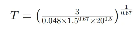
Solving this equation yields (T ≈ 48μm). - Select the nearest standard thickness: 48μm falls between 1oz (35μm) and 1.5oz (52.5μm) copper. 1oz copper is insufficient (as shown in Table 1, a 1.5mm wide 1oz trace can only carry 2.7A), so 1.5oz copper is selected.
- Thermal simulation validation: Using Altium Designer’s thermal simulation tool, the 1.5mm wide 1.5oz trace is simulated to carry 3A with a temperature rise of 18°C—well below the 20°C limit.
- Cost evaluation: 1.5oz copper is 25% more expensive than 1oz copper, but the cost increase is justified by the space savings and compliance with temperature requirements.
5.3 Test Results
The prototype PCB was tested under continuous 3A load for 1000 hours. Key results:
- Average trace temperature rise: 17°C (within the 20°C limit)
- No trace degradation or solder joint failures observed
- PCB footprint reduced by 20% compared to a 1oz copper design with a 2.0mm wide trace
This case study demonstrates how selecting the optimal copper thickness can balance space constraints, performance, and cost for 1–5A power PCBs.
6. Common Mistakes to Avoid in Copper Thickness Selection
Even with clear guidelines, designers often make mistakes that compromise power PCB performance. The following are the most frequent pitfalls and how to avoid them:
- Underestimating current peaks: Many power PCBs experience short-term current peaks (e.g., motor startup currents, capacitor charging currents) that exceed the continuous rating. For 1–5A continuous current PCBs, select copper thickness to handle 1.5–2x the continuous current to accommodate peaks.
- Ignoring internal trace limitations: Designers often use the same copper thickness for internal and external traces, leading to overheating of internal traces. Always reduce the current capacity of internal traces by 30–40% when selecting thickness.
- Prioritizing cost over reliability: Using 1oz copper for 3–5A applications to save costs may lead to premature failures in the field. For applications requiring long-term reliability, the additional cost of thicker copper is a worthwhile investment.
- Neglecting thermal management: Copper thickness alone is not sufficient to ensure low temperature rise. Pair thicker copper with copper pours, heat sinks, and adequate ventilation to maximize heat dissipation.
7. Conclusion
Copper thickness selection for general-purpose power PCBs (1–5A) is a critical design decision that requires balancing current-carrying capacity, thermal performance, cost, and mechanical durability. The IPC-2221 standard provides a quantitative framework for calculating the minimum copper thickness required for a given current and temperature rise, with 1oz, 1.5oz, and 2oz being the standard options for this current range.
Key takeaways for designers include:
- 1oz copper is suitable for 1–2A applications with ample space and moderate reliability requirements.
- 1.5oz copper is ideal for 2–3A applications with space constraints and enhanced reliability needs.
- 2oz copper is necessary for 3–5A applications, compact layouts, or harsh environments (e.g., automotive, industrial).
By following the step-by-step guidelines outlined in this article, validating designs with thermal simulation, and avoiding common pitfalls, engineers can select the optimal copper thickness for 1–5A power PCBs—ensuring reliable, cost-effective, and thermally stable performance across a wide range of applications.