 PCB
PCB FPC
FPC Rigid-Flex
 FR-4
FR-4 HDI PCB
 Rogers High-Frequency Board
 PTFE Teflon High-Frequency Board
 Aluminum
 Copper Core
 PCB Assembly
 LED light PCBA
 Memory PCBA
 Power Supply PCBA
 New Energey PCBA
 Communication PCBA
 Industrial Control PCBA
 Medical Equipment PCBA
 Testing Service
 PCBA Testing Service
 Certification Application
 RoHS Certification Application
 REACH Certification Application
 CE Certification Application
 FCC Certification Application
 CQC Certification Application
 UL Certification Application
 Transformers, Inductors
 High Frequency Transformers
 Low Frequency Transformers
 High Power Transformers
 Conversion Transformers
 Sealed Transformers
 Ring Transformers
 Inductors
 Wires,Cables Customized
 Network Cables
 Power Cords
 Antenna Cables
 Coaxial Cables
 Net Position Indicator
 Solar AIS net position indicator
 Capacitors
 Connectors
 Diodes
 Embedded Processors & Controllers
 Digital Signal Processors (DSP/DSC)
 Microcontrollers (MCU/MPU/SOC)
 Programmable Logic Device(CPLD/FPGA)
 Communication Modules/IoT
 Resistors
 Through Hole Resistors
 Resistor Networks, Arrays
 Potentiometers,Variable Resistors
 Aluminum Case,Porcelain Tube Resistance
 Current Sense Resistors,Shunt Resistors
 Switches
 Transistors
 Power Modules
 Isolated Power Modules
 AC-DC Power Modules
 DC-AC Module(Inverter)
 RF and Wireless
Conventional V-CUT Depth Control Standards
2025-10-09
Conventional V-CUT Depth Control Standards: How to Avoid Over-Cutting and Under-Cutting
1. Core Positioning of V-CUT Process and the Significance of Depth Control
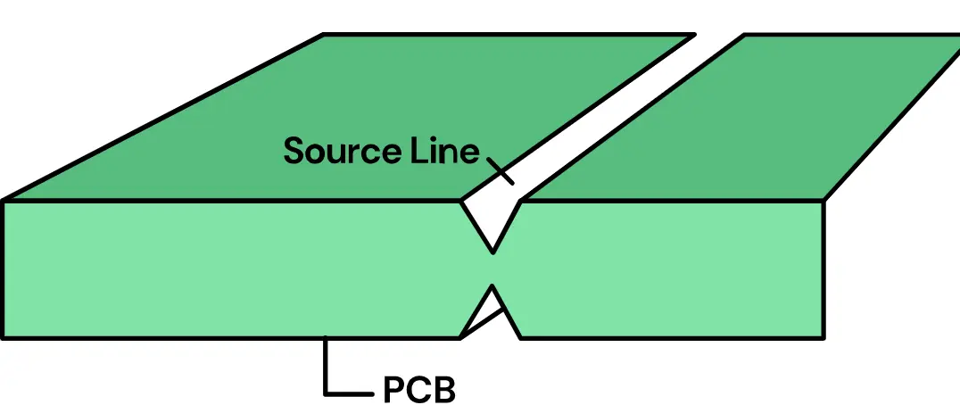
V-CUT (V-groove cutting) is a critICal pre-process for separating multi-panel PCBs. It involves milling symmetrical V-shaped grooves on the front and back sides of the connecting edges of panelized PCBs, leaving a thin central "remaining web" (connecting rib). Later, the panels can be quickly separated along this web using methods like manual snapping or mechanical depaneling machines. This process is widely used for conventional PCBs in consumer electronics, industrial control, and other fields—such as panelized mobile phone motherboards and household appliance control boards.
The core challenge in V-CUT depth control lies in "precision balance": if the depth is too shallow (under-cutting), the remaining web becomes excessively thick. This requires greater force during separation, often resulting in burrs (height > 0.1mm) on PCB edges, circuit deformation, or even delamination. Conversely, if the depth is too deep (over-cutting), the connecting rib is directly severed, causing panels to scatter prematurely during subsequent processes (e.g., SMT mounting, transportation)—pushing defect rates up by more than 20%. Therefore, defining clear V-CUT depth control standards and establishing error-prevention mechanisms is crucial to ensuring Pcb Panel quality and separation efficiency.
2. Conventional V-CUT Depth Control Standards
Conventional V-CUT depth standards are formulated around two core parameters: total PCB thickness and remaining web thickness. These standards also accommodate different V-CUT angles (commonly 30°, 45°, 60°) and substrate types (FR-4, aluminum substrates, etc.). The industry-wide standards are as follows:
2.1 Core Control Indicator: Remaining Web Thickness
The remaining web thickness (hereafter referred to as "remaining thickness") is the "golden indicator" for V-CUT depth control, directly determining separation peRFormance and panel stability. The conventional standard is:
- General Remaining Thickness Range: 0.15–0.3mm, applicable to most PCBs (total thickness 0.8–3.0mm). For example, for a 1.6mm-thick FR-4 PCB, the remaining thickness is controlled at 0.2mm ± 0.02mm. This ensures panels do not scatter during transportation (withstanding 50N of tension without breaking) while enabling easy separation (requiring ≤ 30N of force to snap).
- Remaining Thickness Adjustments for Special Scenarios:
- Thin PCBs (total thickness 0.8–1.2mm): The remaining thickness must be ≥ 0.15mm to avoid insufficient connecting rib strength due to thin substrates. For instance, a 0.8mm-thick PCB requires a remaining thickness of 0.15–0.2mm; if < 0.15mm, the panel may break when adsorbed by SMT nozzles.
- Thick PCBs (total thickness 2.0–3.0mm): The remaining thickness can be relaxed to 0.25–0.3mm. Thick substrates have higher inherent strength, so a slightly thicker web does not hinder separation. For example, a 2.4mm-thick aluminum substrate with a 0.3mm remaining thickness maintains edge flatness within ±0.05mm after separation.
- Flexible PCBs (FPCs): Due to their soft PI substrate, V-CUT remaining thickness must be strictly controlled at 0.15–0.2mm. Special flexible V-CUT tools are also required to prevent breakage during bending caused by uneven remaining thickness.
2.2 Conversion Relationship Between V-CUT Depth and Total Thickness
V-CUT depth (single-sided groove depth) is not a direct measurement but is derived using the formula: Single-sided groove depth = (Total PCB thickness – Remaining web thickness) ÷ 2. This formula applies to conventional symmetrical V-CUT (equal depth on front and back sides). Below are conversion examples for different total thicknesses:
| Total PCB Thickness (mm) | Remaining Web Thickness (mm) | Single-sided Groove Depth (mm) | V-CUT Angle | Application Scenario |
|---|---|---|---|---|
| 1.0 | 0.15–0.2 | 0.4–0.425 | 45° | Thin consumer electronics PCBs (e.g., earphone boards) |
| 1.6 (conventional) | 0.2–0.25 | 0.675–0.7 | 45° | General FR-4 PCBs (e.g., mobile phone motherboards) |
| 2.0 | 0.25–0.3 | 0.85–0.875 | 60° | Thick industrial control boards (e.g., inverter boards) |
| 2.4 (aluminum substrate) | 0.3 | 1.05 | 60° | Power module PCBs (e.g., LED driver boards) |
2.3 Impact of V-CUT Angle on Depth
V-CUT angle (tool angle) indirectly affects depth control accuracy. Matching requirements for conventional angles and depths are as follows:
- 45° Angle (Most Common): Suitable for PCBs with total thickness 0.8–2.0mm. The moderate groove wall inclination simplifies depth deviation control (±0.02mm) and minimizes post-separation edge burrs (≤0.05mm).
- 30° Angle: Used for scenarios requiring "shallow depth and wide groove openings" (e.g., PCBs with components near edges—wide openings prevent tool scratches). Groove depth here should be 0.05–0.1mm shallower than 45° angles to avoid overly thin remaining webs.
- 60° Angle: Ideal for thick boards (>2.0mm). The steep groove walls reduce PCB space occupied by the groove, but depth should be 0.05mm deeper than 45° angles to ensure the remaining web meets standards.
3. Technical Measures to Avoid Over-Cutting and Under-Cutting
Over-cutting (remaining thickness < 0.1mm, or complete severance) and under-cutting (remaining thickness > 0.3mm) primarily stem from "insufficient equipment precision + lack of process monitoring". A four-dimensional prevention system—covering tools, equipment, parameters, and inspection—is required to address these issues:
3.1 Tool Selection and Maintenance: The "First Line of Defense" for Depth Control
- Specialized V-CUT Tools: Use alloy tools (e.g., tungsten steel) with a cutting edge angle matching the design (error ≤ ±1°). Tool diameter should align with PCB thickness (e.g., Φ12mm tools for 1.6mm PCBs). This avoids uneven groove depth caused by angle deviations—for example, a 43° tool (instead of 45°) would reduce depth by 0.03mm, leading to overly thick remaining webs.
- Tool Wear Management: Tools have a service life of 5,000–8,000 meters. Inspect cutting edges every 500 meters (using a 20x microscope); replace tools if edge chips exceed 0.01mm. Worn tools cause depth fluctuations (deviation > ±0.05mm), increasing the risk of local over-cutting or under-cutting.
3.2 Equipment Precision Calibration: The "Core Guarantee" for Stable Depth
- V-CUT Machine Depth Calibration:
- Daily Calibration: Use a standard thickness test board (e.g., 1.6mm FR-4) to adjust tool depth to the theoretical value (e.g., 0.7mm). After processing, measure the remaining thickness—if deviation exceeds ±0.02mm, use the machine’s "depth compensation" function to correct (e.g., increase depth by 0.01mm if remaining thickness is 0.18mm < 0.2mm).
- Weekly Level Calibration: Ensure the V-CUT machine workbench levelness is ≤ 0.02mm/m. Inclined workbenches cause depth deviations across the same board (e.g., 0.05mm/m inclination makes edge depth 0.03mm deeper than the center, risking over-cutting).
- Pressing Mechanism Adjustment: Use a pressure block to secure the PCB during V-CUT (pressure: 0.3–0.5kg/cm²). Excessive pressure dents thin PCBs (increasing over-cutting risk), while insufficient pressure allows PCB movement (causing under-cutting). Adjust pressure based on thickness—slightly higher for thick boards, lower for thin ones.
3.3 Process Parameter Optimization: "Key Details" for Adapting to Different Substrates
- Cutting Speed Control: Conventional speed ranges from 1–3m/min. Speed > 3m/min causes tool vibration (depth deviation ±0.04mm), while speed < 1m/min leads to local overheating and substrate carbonization (especially for FR-4), impairing separation. For example, use 2m/min for 1.6mm FR-4 PCBs and 2.5m/min for aluminum substrates (due to faster heat conduction).
- Layered Cutting Strategy: For thick boards (>2.0mm) or high-Tg substrates (Tg > 180℃), adopt "layered cutting" (2–3 passes, 0.3–0.5mm depth per pass). This avoids excessive tool stress and depth loss from one-time deep cutting. For a 2.4mm-thick PCB, first pass depth = 0.6mm, second pass = 0.45mm—total depth = 1.05mm, remaining thickness = 0.3mm.
3.4 Full-Process Inspection: The "Final Checkpoint" to Prevent Defect Flow
- First Article Inspection (Mandatory): For each batch’s first PCB, conduct three tests:
- Remaining Thickness Measurement: Use a digital micrometer (precision ±0.001mm) to measure three points (both ends and center of the V-CUT edge). Deviation between points must be ≤ 0.03mm; adjust parameters if not.
- Visual Inspection: Use a 10x microscope to check groove wall flatness and edge chipping (≤0.05mm is acceptable). Excessive chipping indicates tool wear or excessive speed.
- Separation Test: Manually snap the first article—qualified panels have no burrs or circuit damage and withstand 30N of tension without breaking before separation.
- In-Process Sampling: Inspect 1 PCB every 100 processed units, focusing on remaining thickness changes. If two consecutive units show >0.03mm deviation, stop production to check tool wear or equipment precision.
- Final Inspection: Use an AOI (Automatic Optical Inspection) system (resolution ≥10μm) to scan V-CUT edges. It automatically identifies over-cut (remaining thickness <0.1mm) or under-cut (remaining thickness >0.3mm) defects with ≥99.5% accuracy.
4. Common V-CUT Depth Anomalies and Solutions
In practice, over-cutting and under-cutting often result from parameter deviations or equipment issues. Targeted troubleshooting is required:
| Anomaly | Typical Symptom | Root Cause | Solution |
|---|---|---|---|
| Local Over-Cutting | Section of V-CUT edge has remaining thickness <0.1mm or breaks | 1. Foreign matter (e.g., solder dross) on the workbench lifts the PCB locally; 2. Local tool wear (edge chips) | 1. Clean the workbench with alcohol and verify flatness; 2. Replace the tool and test with a sample board before resuming production |
| Overall Over-Cutting | Entire V-CUT edge has remaining thickness <0.1mm | 1. Incorrect depth parameter settings (e.g., 0.8mm groove depth for 1.6mm PCBs); 2. Excessive pressing pressure dents the PCB | 1. Recheck parameters using the "total thickness – remaining thickness" formula; 2. Reduce pressing pressure to 0.3kg/cm² |
| Overall Under-Cutting | Remaining thickness >0.3mm; excessive force needed to separate | 1. Insufficient depth (parameters set too shallow); 2. Tool angle deviation (e.g., 50° instead of 45°) | 1. Increase depth by 0.05mm and retest remaining thickness; 2. Replace with a correctly angled tool and calibrate equipment |
| Uneven Remaining Thickness | >0.05mm deviation across the same board | 1. Loose equipment guide rails cause tool tilt during movement; 2. Uneven PCB substrate thickness (deviation >0.05mm) | 1. Tighten guide rail screws and calibrate tool movement precision; 2. Replace substrates with thickness deviation ≤0.03mm |