 PCB
PCB FPC
FPC Rigid-Flex
 FR-4
FR-4 HDI PCB
 Rogers High-Frequency Board
 PTFE Teflon High-Frequency Board
 Aluminum
 Copper Core
 PCB Assembly
 LED light PCBA
 Memory PCBA
 Power Supply PCBA
 New Energey PCBA
 Communication PCBA
 Industrial Control PCBA
 Medical Equipment PCBA
 Testing Service
 PCBA Testing Service
 Certification Application
 RoHS Certification Application
 REACH Certification Application
 CE Certification Application
 FCC Certification Application
 CQC Certification Application
 UL Certification Application
 Transformers, Inductors
 High Frequency Transformers
 Low Frequency Transformers
 High Power Transformers
 Conversion Transformers
 Sealed Transformers
 Ring Transformers
 Inductors
 Wires,Cables Customized
 Network Cables
 Power Cords
 Antenna Cables
 Coaxial Cables
 Net Position Indicator
 Solar AIS net position indicator
 Capacitors
 Connectors
 Diodes
 Embedded Processors & Controllers
 Digital Signal Processors (DSP/DSC)
 Microcontrollers (MCU/MPU/SOC)
 Programmable Logic Device(CPLD/FPGA)
 Communication Modules/IoT
 Resistors
 Through Hole Resistors
 Resistor Networks, Arrays
 Potentiometers,Variable Resistors
 Aluminum Case,Porcelain Tube Resistance
 Current Sense Resistors,Shunt Resistors
 Switches
 Transistors
 Power Modules
 Isolated Power Modules
 AC-DC Power Modules
 DC-AC Module(Inverter)
 RF and Wireless
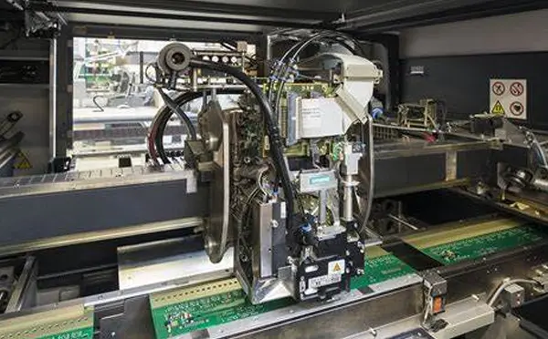
Detailed Explanation of Allowable Placement Offset for SMT Components
- Minor offset (near the threshold): May result in uneven solder volume (more on one side, less on the other), affecting mechanical strength;
- Severe offset (exceeding the threshold): Can lead to pin bridging (short circuit), cold soldering (pins not covered by solder paste), or even component detachment. Industry statistics show that approximately 20% of SMT soldering defects are caused by placement offset.
- Definition: The deviation of the component’s center from the designed coordinates along the X-axis (horizontal direction) or Y-axis (vertical direction), measured in mm. The allowable range is defined by "the ratio of pad width/length" or "absolute dimension" (priority is given to the ratio to ensure adaptation to different pad specifications).
- General Rules:
- Chip components (0603, 0805, 1206, etc.): Allowable offset ≤ 1/3 of the pad width (or ≤ 1/3 of the pad length, whichever is smaller), and absolute offset ≤ 0.2mm (to prevent excessive offset caused by ratio calculation for small pads);
- Lead-containing components (SOIC, QFP, etc.): Allowable offset ≤ 1/2 of the pin width, and it is required that "the solder paste coverage area of the pin ≥ 75%" (if the pin is only 50% covered by solder paste, it is judged as unqualified even if the offset ≤ 1/2).
- Definition: The angular deviation of the component rotating around its center, measured in ° (degrees), which mainly affects lead-containing components (rotational offset of chip components has little impact on soldering).
- General Rules:
- Chip components (0603 and larger): Allowable rotational offset ≤ 10° (since chip components have no obvious pins, solder can still cover the pads when rotated within 10°);
- Lead-containing components (SOIC, QFP): Allowable rotational offset ≤ 5° (the smaller the pin pitch, the smaller the allowable rotational angle; e.g., QFP with a pin pitch of 0.5mm has a rotational offset ≤ 3°), and it is required that "no pin extends beyond the pad edge" (if the pin extends beyond the pad after rotation, it is judged as unqualified even if the angle ≤ 5°).
- Core Characteristics: No independent pins; soldering relies on end electrodes and pads. Offset mainly affects the contact area between end electrodes and pads.
- Allowable Range (IPC-A-610 Class 2, Conventional Scenarios):
- Special Note: For high-reliability scenarios (IPC Class 3, e.g., medical equipment), the standard shall be tightened—linear offset ≤ 1/4 of the pad width, rotational offset ≤ 8°, and end electrode coverage ≥ 80%—to avoid poor contact in extreme environments.
- Core Characteristics: With independent pins (quantity ≥ 8). Offset easily causes pins to extend beyond pads (short-circuit risk), so the alignment between pins and pads must be strictly controlled.
- Allowable Range (Equivalent Size of 0603 and Larger, e.g., SOIC-8, QFP-16):
- Key Logic: The smaller the pin pitch, the narrower the allowable range of linear and rotational offsets—for example, a QFP with a pin pitch of 0.5mm (65% smaller than SOIC’s 1.27mm) has a linear offset tightened from 0.15mm to 0.08mm to prevent pin bridging (a slight offset may cause a short circuit due to small pitch).
- Core Characteristics: Irregular structure (e.g., SOT-23 with 3 pins, XT60 with 2 large terminals). The allowable offset range shall be combined with "terminal/pin size" and "functional requirements" (e.g., connectors need to ensure plug-in alignment).
- Allowable Range (Equivalent Volume of 0603 and Larger):
- Special Requirement: For connector components (e.g., XT60), due to subsequent plug-in operations, the allowable linear offset range is wider than that of chip components (0.38mm vs 0.1mm), but the rotational offset is strict (≤ 3°) to prevent terminal misalignment and plug-in failure.
- Tools: 10-20x magnifying glass (routine inspection), 3D placement inspection machine (mass production, accuracy ±0.01mm);
- Steps:
- Alignment Benchmark: Use the component silkscreen frame on the PCB as the benchmark (the silkscreen frame is concentric with the pad, deviation ≤ 0.05mm), and observe the gap between the component edge and the silkscreen frame;
- Offset Measurement: If the component edge extends beyond the silkscreen frame, use a caliper to measure the extension distance (i.e., offset) and compare it with the allowable range;
- Coverage Verification: Observe the overlapping area between the component’s end electrodes/pins and the pad to ensure the coverage ratio meets the standard (e.g., ≥ 70%).
- Low-Risk Offset (Exceeding the Allowable Range by ≤ 0.05mm, e.g., 0603 offset 0.12mm, exceeding by 0.02mm):
- Medium-Risk Offset (Exceeding the Allowable Range by 0.05-0.1mm, e.g., 0805 offset 0.18mm, exceeding by 0.06mm):
- High-Risk Offset (Exceeding the Allowable Range by > 0.1mm, e.g., QFP offset 0.2mm, exceeding by 0.12mm):
- Consequence: For example, if the 0603 pad width is 0.25mm (non-standard 0.3mm), judging by the absolute dimension of 0.1mm (1/3 × 0.25mm ≈ 0.08mm), an offset of 0.09mm will be mistakenly judged as qualified, but it actually exceeds the ratio;
- Avoidance: Calculate based on "1/3 of the pad width" first, then take the smaller value with "absolute dimension of 0.2mm" to ensure double restriction.
- Consequence: For example, if an SOIC-8 rotates by 6° (exceeding the allowable 5°) and has a linear offset of 0.1mm (qualified), the pins have extended beyond the pad edge, leading to a short circuit after soldering;
- Avoidance: During placement inspection, first check the rotational offset (visually observe whether the component is "tilted"), then measure the linear offset. If the rotational offset exceeds the range, directly judge as unqualified.
- Consequence: A 0603 resistor in medical equipment is judged according to the conventional Class 2 standard (offset ≤ 0.1mm), but it actually requires Class 3 (≤ 0.075mm), posing reliability risks;
- Avoidance: Determine the IPC class based on the product application scenario (Class 2 for consumer electronics, Class 3 for medical/aerospace), and then adjust the allowable offset range accordingly.
- Size Adaptation: The larger the component size (e.g., 2010 vs 0603) and the wider the pin pitch (e.g., SOIC 1.27mm vs QFP 0.5mm), the wider the allowable offset range;
- Function Priority: The offset range of components in critical circuits (power supply, signal transmission) is narrower than that in non-critical circuits (indicator lights), and the range in high-reliability scenarios is narrower than that in conventional scenarios;
- Soldering Guarantee: The bottom line of all allowable ranges is that "the end electrode/pin coverage of the component on the solder paste ≥ 60%" and there is no short-circuit risk (pins do not extend beyond pads).
7. Summary and Design Recommendations
The allowable range for SMT component placement offset is a comprehensive quality requirement, whose core standards are clearly defined in IPC-A-610: For 0603 and larger rectangular components, typically at least 50% of the termination width must overlap the pad (Class 1/2), while high-reliability products (Class 3) require this to be increased to 75%. For ICs and BGAs, the rules are stricter, usually requiring 3/4 or more of the lead or solder ball to be on the pad, and the center offset of BGA solder balls needs to be less than their radius.
To ensure your design meets these requirements, the following is recommended:
-
Focus on Both Design and Process: Excellent pad design (complying with IPC standards) is the foundation, while refined process control is the guarantee for realizing the design intent.
-
Utilize Tools Effectively: Actively use DFM analysis tools (e.g., Huaqiu DFM) to check the rationality of pad design during the design stage.
-
Process Monitoring: Rely on tools like AOI and SPC for continuous monitoring and feedback during production, forming a closed-loop quality management system.
-
Standard Selection: Always select the appropriate acceptance Class based on the product's end-use and establish stricter corporate standards when necessary in communication with customers.
Understanding and applying these standards and control methods can significantly improve SMT yield and ultimately ensure the reliability and service life of electronic products.