 PCB
PCB FPC
FPC Rigid-Flex
 FR-4
FR-4 HDI PCB
 Rogers High-Frequency Board
 PTFE Teflon High-Frequency Board
 Aluminum
 Copper Core
 PCB Assembly
 LED light PCBA
 Memory PCBA
 Power Supply PCBA
 New Energey PCBA
 Communication PCBA
 Industrial Control PCBA
 Medical Equipment PCBA
 Testing Service
 PCBA Testing Service
 Certification Application
 RoHS Certification Application
 REACH Certification Application
 CE Certification Application
 FCC Certification Application
 CQC Certification Application
 UL Certification Application
 Transformers, Inductors
 High Frequency Transformers
 Low Frequency Transformers
 High Power Transformers
 Conversion Transformers
 Sealed Transformers
 Ring Transformers
 Inductors
 Wires,Cables Customized
 Network Cables
 Power Cords
 Antenna Cables
 Coaxial Cables
 Net Position Indicator
 Solar AIS net position indicator
 Capacitors
 Connectors
 Diodes
 Embedded Processors & Controllers
 Digital Signal Processors (DSP/DSC)
 Microcontrollers (MCU/MPU/SOC)
 Programmable Logic Device(CPLD/FPGA)
 Communication Modules/IoT
 Resistors
 Through Hole Resistors
 Resistor Networks, Arrays
 Potentiometers,Variable Resistors
 Aluminum Case,Porcelain Tube Resistance
 Current Sense Resistors,Shunt Resistors
 Switches
 Transistors
 Power Modules
 Isolated Power Modules
 AC-DC Power Modules
 DC-AC Module(Inverter)
 RF and Wireless
Comparison of Flying Probe Test vs. Bed of Nails Test: Pros and Cons
Comparison of Flying Probe Test vs. Bed of Nails Test: Pros and Cons
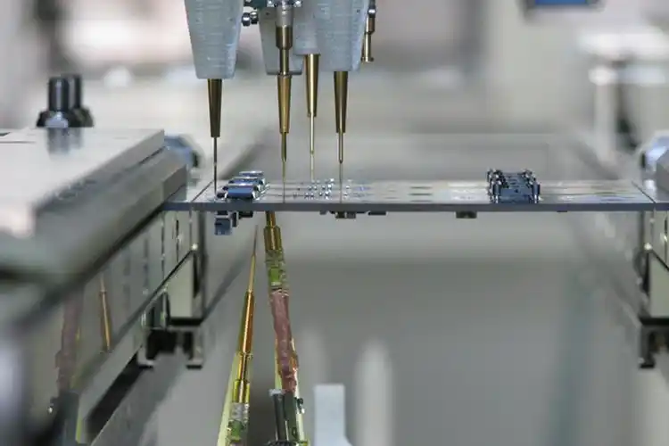
Flying Probe Test
Advantages:
-
High Flexibility
-
No custom fixtures required, ideal for low-volume production, prototypes, or designs with frequent changes.
-
Adaptable to PCBs of varying sizes and complexities, with easy adjustment of test point locations.
-
-
Low Initial Cost
-
Eliminates fixture fabrICation costs, making it cost-effective for R&D or low-volume production.
-
High Test Coverage
-
Dynamic probe movement supports complex routing and high-density component testing.
-
-
Easy Maintenance
-
Probes are SIMple to replace and calibrate, with no physical fixture wear.
-
Disadvantages:
-
Slow Testing Speed
-
Sequential probe movement leads to longer test times, unsuitable for high-volume production.
-
-
Limited Contact Pressure
-
Lower probe pressure may affect accuracy for high-impedance or low-level signal testing.
-
-
Limited Parallel Testing
-
Typically tests one PCB at a time, reducing throughput.
-
Bed of Nails Test
Advantages:
-
Fast Testing Speed
-
Simultaneous contact with all test points via a fixture enables high-volume production efficiency.
-
-
Stable Contact
-
Spring-loaded pins ensure reliable connections, critical for high-frequency or high-current testing.
-
-
Parallel Testing Support
-
Fixtures can be designed for multi-board testing, enhancing productivity.
-
-
Long-Term Cost Efficiency
-
Lower per-unit testing cost for large volumes due to amortized fixture costs.
-
Disadvantages:
-
High Initial Cost
-
Custom fixtures are expensive and time-consuming (weeks to design), unsuitable for small batches or iterative designs.
-
-
Low Flexibility
-
Design changes require new fixtures, increasing time and cost.
-
-
Physical Limitations
-
High-density or miniaturized PCBs may face challenges with test point spacing.
-
-
Complex Maintenance
-
Fixture pins are prone to wear, deformation, or contamination, requiring regular upkeep.
-
Summary Comparison
| Feature | Flying Probe Test | Bed of Nails Test |
|---|---|---|
| Applicability | Low-volume, prototypes, complex PCBs | High-volume, mature designs, standard PCBs |
| Initial Cost | Low (no fixtures) | High (custom fixtures) |
| Testing Speed | Slow | Fast |
| Flexibility | High | Low |
| Long-Term Cost | High per-unit (time cost) | Low per-unit (amortized fixtures) |
| Maintenance | Simple | Complex |
Evaluating PCB Long-Term Reliability via Accelerated Aging Tests
1. Principles of Accelerated Aging
By applying environmental stresses (e.g., temperature, humidity, vibration) beyond normal operating conditions, material degradation or failure mechanisms are accelerated, enabling prediction of long-term reliability in shorter timeframes.
2. Common Accelerated Aging Methods
a. Thermal Cycling Test
-
Method: Expose PCBs to extreme temperature cycles (e.g., -40°C to +125°C) to simulate thermal stress from power cycling or environmental changes.
-
Purpose: Evaluate solder joint fatigue, CTE mismatch-induced delamination, or layer cracking.
-
Key Parameters: Temperature range, cycle count, ramp rate (e.g., 10°C/min).
b. Temperature Humidity Bias (THB) Test
-
Method: Subject PCBs to high humidity and temperature (e.g., 85°C/85% RH) under electrical bias to accelerate conductive anodic filament (CAF) growth or insulation resistance degradation.
-
Purpose: Detect metal migration (e.g., dendrites), CAF formation, or insulation failures.
-
Key Parameters: Temperature/humidity levels, bias voltage, duration (e.g., 1,000 hours).
c. Highly Accelerated Life Test (HALT)
-
Method: Apply escalating stresses (rapid thermal changes, multi-axis vibration, voltage spikes) until failure occurs.
-
Purpose: Identify design weaknesses and determine operational/destructive limits.
-
Key Parameters: Stress types, step increments, failure criteria.
d. High-Temperature Storage Test
-
Method: Store PCBs at elevated temperatures (e.g., 150°C) to accelerate oxidation or material degradation.
-
Purpose: Assess long-term material stability under thermal stress.
3. Data Analysis and Reliability Modeling
a. Failure Data Collection
-
Document failure modes (e.g., opens, shorts, parametric drift) and timelines.
-
Use microscopy, X-ray, or SEM/EDS for root cause analysis (e.g., solder cracks, CAF).
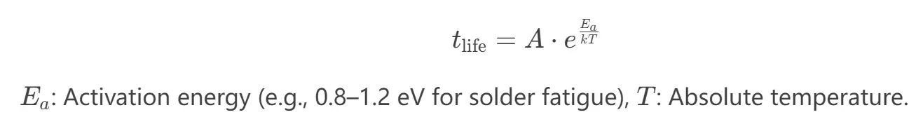
b. Reliability Modeling
-
Arrhenius Model: Predicts temperature-accelerated lifespan:
-
Weibull Distribution: Analyzes failure probability:

c. Acceleration Factor (AF) Calculation
-
Temperature AF:
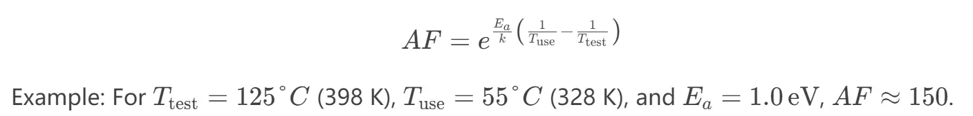
-
Equivalent Lifetime:
Actual Lifetime=Test Duration
4. Standards and Guidelines
-
IPC-9701: Thermal cycling standards for PCB assemblies.
-
JEDEC JESD22-A101: Steady-state humidity reliability testing.
-
IEC 60068-2-14: Temperature variation testing methodology.
5. Case Study: Automotive PCB Reliability Validation
-
Test Design:
-
Thermal cycling: -40°C to +125°C, 1,000 cycles (simulating 10-year in-vehicle use).
-
THB: 85°C/85% RH, 1,000 hours with 5V bias.
-
-
Findings:
-
Solder joint cracks (thermal cycling) → Optimized solder paste.
-
CAF between adjacent vias (THB) → Improved solder mask process.
-
-
Outcome: Validated 15-year reliability for automotive applications post-design refinements.