Common PCB SuRFace Treatment Processes and Their Application Scenarios
- HASL (Hot Air Solder Leveling)
Process Characteristics: The PCB is immersed in molten tin - lead (or lead - free tin), and then hot air is used to scrape the surface to form a uniform tin layer.
Application Scenarios:
- Low - cost applications: Consumer electronics (such as home appliances, toys), ordinary coMPUter motherboards.
- Through - hole Technology (THT): Suitable for through - hole components that require good solder wettability.
- Non - high - density designs: The requirement for surface flatness is not high, and it is not suitable for fine - pitch BGA or QFN packages.
Advantages: Low cost, good soldering performance, and resistant to storage.
Disadvantages: Uneven surface, non - uniform tin layer thickness, and not suitable for high - density designs.
- ENIG (Electroless Nickel Immersion Gold)
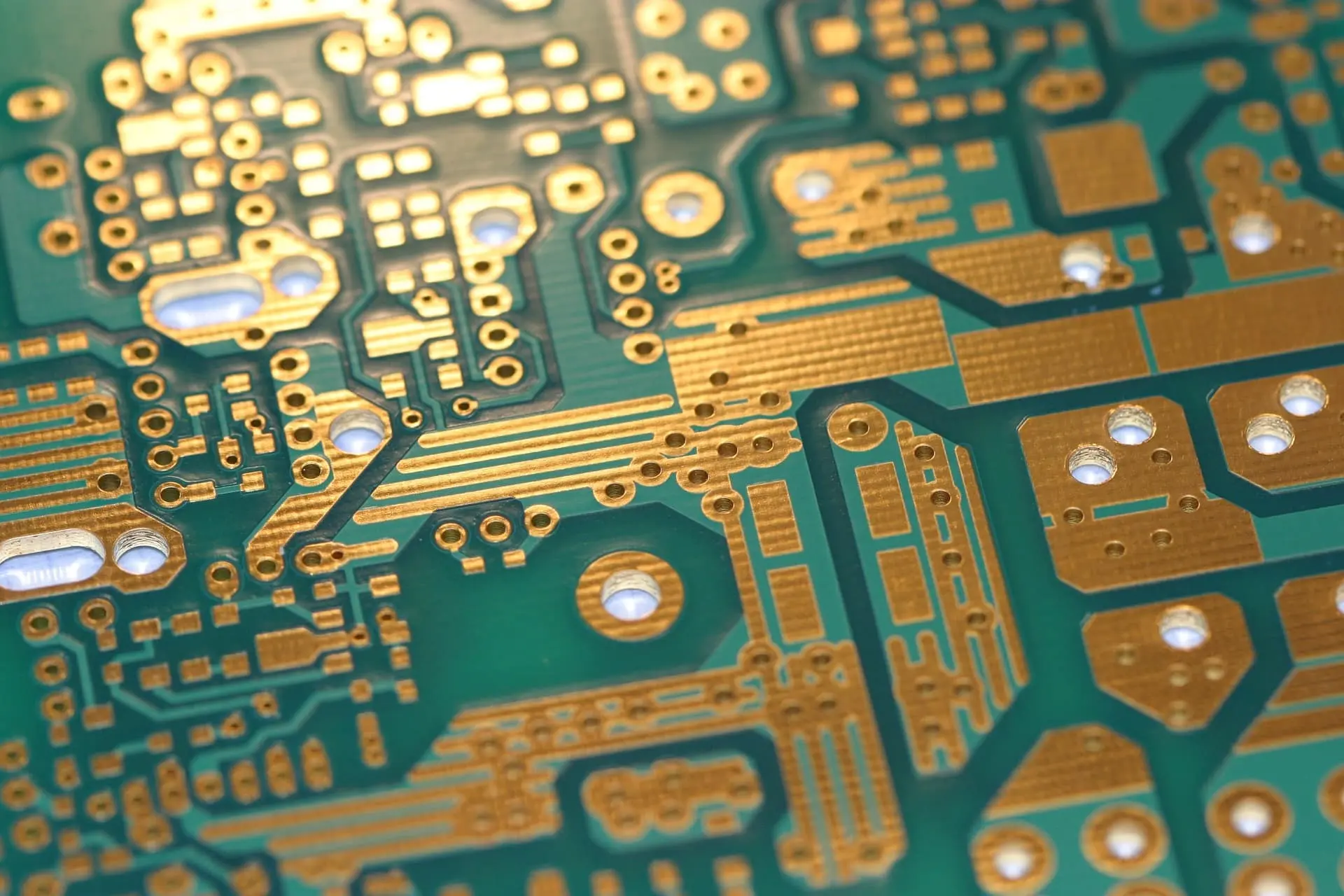
Process Characteristics: After electroless nickel plating (5 - 8 μm) on the copper surface, gold is immersed (0.05 - 0.2 μm) to form a flat nickel - gold layer.
Application Scenarios:
- High - Density Interconnect (HDI): Smartphones, tablets, server motherboards.
- Multiple reflow soldering: Suitable for SMT processes that require multiple assembly operations.
- Gold - finger connectors: Provide low contact resistance and wear resistance.
- High - frequency/high - speed signals: The nickel layer can shield electromagnetic interference (EMI).
Advantages: Flat surface, oxidation - resistant, and suitable for fine - pitch components.
Disadvantages: High cost, prone to the "Black Pad" effect.
- OSP (Organic Solderability Preservative)
Process Characteristics: A layer of organic protective film is coated on the copper surface to prevent oxidation.
Application Scenarios:
- Short - cycle production: Fast - turnaround consumer electronics products (such as routers, LED lights).
- Lead - free soldering: Scenarios with strict environmental protection requirements (compliant with RoHS).
- Low - cost SMT: Simple designs where the surface does not require complex treatment.
Advantages: The lowest cost, environmentally friendly, and simple process.
Disadvantages: The protective film is easily affected by moisture/scratches, and it is not suitable for long - term storage or multiple soldering.
Supplementary Information on Other Common Processes:
- Immersion Silver: Suitable for high - frequency circuits (such as RF modules), but it is prone to sulfidation and blackening.
- ENEPIG (Electroless Nickel Electroless Palladium Immersion Gold): A high - reliability process to replace ENIG, suitable for aerospace or automotive electronics.
Causes of the "Black Pad" Effect in the ENIG Process
The "Black Pad" effect is a local corrosion phenomenon that occurs at the interface of the nickel - gold layer in the ENIG process. It is manifested as the blackening of the pad surface, a decrease in welding strength, and even detachment. Its root causes are closely related to the quality of the nickel layer and process control:
- Corrosion Mechanism of the Nickel Layer
- Uneven phosphorus content: During electroless nickel plating, the distribution of phosphorus in the nickel - phosphorus alloy is uneven (normal content: 7 - 10%). High - phosphorus regions are prone to forming an amorphous structure, while low - phosphorus regions are crystalline. Crystalline nickel is preferentially corroded in the gold - immersion solution (strong oxidizing property), leading to micro - cracks.
- Over - corrosion: The gold - immersion solution (usually containing thiourea or cyanide) overly attacks the nickel layer, forming a porous and loose phosphorus - rich layer (black nickel).
- Failure of Process Control
- Plating solution contamination: Contamination of copper ions (Cu²⁺) in the nickel tank leads to a displacement reaction, generating a loose copper - nickel layer.
- Temperature/pH fluctuations: Unstable temperature or pH value of the nickel plating solution affects the compactness of the coating.
- Too thin gold layer: Insufficient gold - immersion time results in a gold layer (<0.05 μm) that cannot completely cover the nickel layer, and the exposed nickel oxidizes during soldering.
- Interface Diffusion Problems
- Nickel - gold interface diffusion: During high - temperature soldering, nickel atoms diffuse into the gold layer, causing the formation of brittle intermetallic compounds (such as Ni₃Au) at the interface, reducing the bonding strength.
Preventive Measures for the "Black Pad" Effect
- Optimize the plating solution formula: Control the phosphorus content in the nickel tank (7 - 10%) and avoid copper - ion contamination.
- Strictly control process parameters: Stabilize the plating solution temperature (85 - 90°C), pH value (4.5 - 5.2), and gold - immersion time (5 - 8 minutes).
- Strengthen gold - layer protection: Ensure that the gold - layer thickness is ≥0.1 μm to reduce the risk of nickel exposure.
- Post - treatment inspection: Analyze the compactness of the nickel layer through cross - section analysis or SEM/EDS detection.
 PCB
PCB FPC
FPC Rigid-Flex
 FR-4
FR-4 HDI PCB
 Rogers High-Frequency Board
 PTFE Teflon High-Frequency Board
 Aluminum
 Copper Core
 PCB Assembly
 LED light PCBA
 Memory PCBA
 Power Supply PCBA
 New Energey PCBA
 Communication PCBA
 Industrial Control PCBA
 Medical Equipment PCBA
 Testing Service
 PCBA Testing Service
 Certification Application
 RoHS Certification Application
 REACH Certification Application
 CE Certification Application
 FCC Certification Application
 CQC Certification Application
 UL Certification Application
 Transformers, Inductors
 High Frequency Transformers
 Low Frequency Transformers
 High Power Transformers
 Conversion Transformers
 Sealed Transformers
 Ring Transformers
 Inductors
 Wires,Cables Customized
 Network Cables
 Power Cords
 Antenna Cables
 Coaxial Cables
 Net Position Indicator
 Solar AIS net position indicator
 Capacitors
 Connectors
 Diodes
 Embedded Processors & Controllers
 Digital Signal Processors (DSP/DSC)
 Microcontrollers (MCU/MPU/SOC)
 Programmable Logic Device(CPLD/FPGA)
 Communication Modules/IoT
 Resistors
 Through Hole Resistors
 Resistor Networks, Arrays
 Potentiometers,Variable Resistors
 Aluminum Case,Porcelain Tube Resistance
 Current Sense Resistors,Shunt Resistors
 Switches
 Transistors
 Power Modules
 Isolated Power Modules
 AC-DC Power Modules
 DC-AC Module(Inverter)
 RF and Wireless