 PCB
PCB FPC
FPC Rigid-Flex
 FR-4
FR-4 HDI PCB
 Rogers High-Frequency Board
 PTFE Teflon High-Frequency Board
 Aluminum
 Copper Core
 PCB Assembly
 LED light PCBA
 Memory PCBA
 Power Supply PCBA
 New Energey PCBA
 Communication PCBA
 Industrial Control PCBA
 Medical Equipment PCBA
 Testing Service
 PCBA Testing Service
 Certification Application
 RoHS Certification Application
 REACH Certification Application
 CE Certification Application
 FCC Certification Application
 CQC Certification Application
 UL Certification Application
 Transformers, Inductors
 High Frequency Transformers
 Low Frequency Transformers
 High Power Transformers
 Conversion Transformers
 Sealed Transformers
 Ring Transformers
 Inductors
 Wires,Cables Customized
 Network Cables
 Power Cords
 Antenna Cables
 Coaxial Cables
 Net Position Indicator
 Solar AIS net position indicator
 Capacitors
 Connectors
 Diodes
 Embedded Processors & Controllers
 Digital Signal Processors (DSP/DSC)
 Microcontrollers (MCU/MPU/SOC)
 Programmable Logic Device(CPLD/FPGA)
 Communication Modules/IoT
 Resistors
 Through Hole Resistors
 Resistor Networks, Arrays
 Potentiometers,Variable Resistors
 Aluminum Case,Porcelain Tube Resistance
 Current Sense Resistors,Shunt Resistors
 Switches
 Transistors
 Power Modules
 Isolated Power Modules
 AC-DC Power Modules
 DC-AC Module(Inverter)
 RF and Wireless
Distinguishing Between Cold Solder Joints Caused by Insufficient Temperature and Poor Solder Quality on a PCBA
2026-01-05

Cold solder joints are one of the most common and troublesome defects in printed Circuit Board assembly (PCBA) manufacturing. A cold solder joint is defined as a solder connection that fails to form a proper metallurgical bond between the component lead/pin and the PCB pad, typically due to incomplete solder melting, inadequate wetting, or improper solidification. This defect compromises the electrical conductivity, mechanical strength, and long-term reliability of the PCBA, often leading to intermittent failures, signal degradation, or complete circuit breakdown. While cold solder joints can stem from multiple root causes, two of the most prevalent are insufficient soldering temperature and poor solder quality. Distinguishing between these two causes is critical for implementing targeted corrective actions, optimizing the soldering process, and preventing recurrence.
Insufficient soldering temperature occurs when the heat applied during soldering (either from a soldering iron, reflow oven, or wave soldering machine) is not high enough to fully melt the solder alloy, activate the flux, and facilitate proper wetting of the component lead and pad. Poor solder quality, on the other hand, refers to defects in the solder material itself—such as incorrect alloy composition, contamination, expired flux, or improper particle size distribution—that prevent the formation of a sound joint even when soldering parameters are optimal. The challenge in distinguishing these causes lies in the fact that both can produce cold solder joints with SIMilar initial appearances. However, through a systematic approach combining visual inspection, physical and electrical testing, chemical analysis, and process traceability, manufacturers can accurately identify whether the root cause is temperature-related or a result of substandard solder.
Foundational Understanding: Cold Solder Joint Formation Mechanisms
To effectively distinguish between temperature- and solder quality-induced cold joints, it is first essential to understand the metallurgical and chemical processes that underpin proper solder joint formation—and how these processes fail in each scenario.
Proper Solder Joint Formation
A high-quality solder joint forms through three key stages: flux activation, solder melting and wetting, and solidification. Flux, a critical component of solder wire or paste, removes oxide layers from the component lead and PCB pad, cleans the surfaces, and reduces surface tension to enable solder flow. When sufficient heat is applied, the solder alloy melts (at a temperature specific to its composition, e.g., 183°C for Sn63/Pb37, 217°C for SAC305 lead-free solder) and wets the cleaned metal surfaces. Wetting is the process by which molten solder spreads uniformly across the pad and lead, forming a continuous, concave fillet and establishing a metallurgical intermetallic compound (IMC) layer between the solder and the base metal (e.g., copper). This IMC layer is essential for mechanical strength and electrical conductivity. As the solder cools and solidifies, it retains the fillet shape, creating a robust joint.
Cold Joint Formation Due to Insufficient Temperature
When soldering temperature is insufficient (either below the solder’s melting point or just above it but without enough dwell time), the solder fails to fully melt or wet the surfaces. Flux may not activate completely, leaving oxide layers intact and preventing proper metal-to-metal contact. The solder may partially melt, forming a grainy, uneven fillet, or it may solidify prematurely before wetting can occur. In some cases, the solder may adhere to the lead or pad but not both, resulting in a weak mechanical bond and poor electrical continuity. The IMC layer, if formed at all, is thin, discontinuous, or nonexistent. This type of cold joint is typically process-dependent, affecting multiple joints on a PCBA or across a production batch if the temperature issue is systemic (e.g., a malfunctioning reflow oven zone).
Cold Joint Formation Due to Poor Solder Quality
Poor solder quality disrupts the soldering process even when temperature and other parameters are correct. Common solder quality issues include: incorrect alloy composition (e.g., too high a percentage of impurities that raise the melting point), flux contamination or expiration (reducing its cleaning and wetting capabilities), solder oxidation (forming a surface oxide layer that inhibits melting), or inconsistent particle size (for solder paste, leading to uneven melting). For example, expired flux may lose its ability to remove oxides, even at the correct temperature, resulting in poor wetting and cold joints. Contaminated solder (e.g., with dirt, moisture, or foreign metals) can cause inconsistent melting and solidification, leading to grainy, brittle joints. Unlike temperature-induced cold joints, solder quality issues may affect specific batches of solder, regardless of the PCBA or production line, and may appear randomly across a batch if the solder is unevenly contaminated.
Step 1: Visual and Macroscopic Inspection – Initial Differentiation Clues
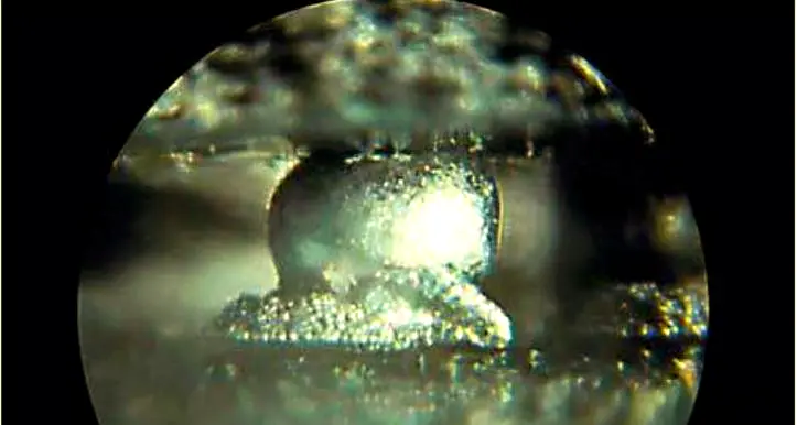
Visual and macroscopic inspection (using a stereomicroscope with 10-50x magnification) is the first step in distinguishing between temperature- and solder quality-related cold joints. While both types share some common cold joint characteristics (e.g., dull appearance, irregular fillets), they also exhibit distinct features that provide initial clues about the root cause.
Common Cold Joint Visual Characteristics (Shared by Both Causes)
Regardless of whether the cause is temperature or solder quality, cold joints typically display the following features:
- Dull, matte finish: Unlike the smooth, shiny surface of a properly formed solder joint (resulting from uniform solidification), cold joints have a grainy, dull appearance due to rapid or uneven solidification.
- Irregular fillet shape: The solder fillet (the curved area between the component lead and pad) may be incomplete, concave, or jagged, rather than the ideal smooth, convex shape.
- Solder pullback: The solder may pull away from the pad or lead, leaving gaps or exposed metal surfaces.
- Cracks or voids: Small cracks or voids may be visible in the solder joint, indicating poor cohesion during solidification.
Temperature Insufficiency-Specific Visual Clues
Cold joints caused by insufficient temperature often exhibit patterns and features related to incomplete heat transfer and premature solidification:
1. Patterned distribution: Temperature-induced cold joints tend to cluster in specific areas of the PCBA. For example, joints on large thermal mass components (e.g., connectors, heat sinks) or on the edges of the PCB (which may cool faster in a reflow oven) are more likely to be cold if temperature is insufficient. Similarly, all joints on a batch of PCBs processed in a reflow oven with a malfunctioning heating zone may show cold joint characteristics.
2. Partial melting signs: The solder may appear partially melted, with visible solid solder particles embedded in a molten matrix. This is particularly common in solder paste applications, where insufficient temperature prevents full melting of the solder particles.
3. Flux residue anomalies: Flux residue may be excessive, sticky, or discolored (e.g., brown or black), indicating incomplete activation. Insufficient temperature prevents the flux from fully evaporating or decomposing, leaving behind unreacted residue that can interfere with wetting.
4. Lack of wetting on specific surfaces: The solder may wet one surface (e.g., the component lead) but not the other (e.g., the PCB pad), indicating that heat was not evenly distributed to both surfaces. For example, if a soldering iron tip only contacts the lead and not the pad, the pad remains too cool for proper wetting.
Solder Quality-Specific Visual Clues
Cold joints caused by poor solder quality often exhibit features related to material defects, rather than process distribution:
1. Random distribution: Unlike temperature-induced cold joints, those caused by poor solder quality are often randomly distributed across a PCBA or production batch. For example, some joints on a single PCB may be sound, while others are cold, depending on how the defective solder was applied (e.g., uneven flux distribution in solder paste).
2. Solder oxidation: The solder surface may have a thick, dark oxide layer (gray or black), even after soldering. This indicates that the solder was oxidized before or during soldering (e.g., due to poor packaging, moisture absorption, or expired shelf life), preventing proper melting and wetting.
3. Flux-related defects: Flux may be absent, dried out, or contaminated. For example, expired solder wire may have flux that is hard and non-reactive, leading to poor cleaning and wetting. Contaminated flux may leave crystalline or powdery residue on the joint.
4. Inconsistent solder texture: The solder may have a brittle, crumbly texture, with visible voids or inclusions (e.g., dirt, metal particles). This is common in solder with incorrect alloy composition or contamination, which disrupts uniform solidification.
Step 2: Physical and Mechanical Testing – Evaluating Joint Integrity
Physical and mechanical testing helps further differentiate between temperature- and solder quality-induced cold joints by evaluating the strength and cohesion of the solder joint. Temperature-induced cold joints typically fail due to poor wetting and incomplete IMC formation, while solder quality-induced joints fail due to material defects (e.g., brittleness, contamination).
Pull Test and Shear Test
Pull and shear tests measure the force required to separate the component lead from the PCB pad, providing insights into joint strength. These tests are typically performed using specialized equipment (e.g., a universal testing machine) with a load cell to measure force accurately.
• Temperature insufficiency: Cold joints from insufficient temperature have low shear and pull strength due to incomplete wetting and lack of a continuous IMC layer. When tested, the joint often fails at the interface between the solder and the pad/lead (adhesive failure), with little or no solder remaining on the pad. The failure surface is typically smooth, indicating poor adhesion.
• Poor solder quality: Cold joints from poor solder quality also have low strength, but the failure mode is different. The joint often fails within the solder itself (cohesive failure), with solder remaining on both the pad and lead. The failure surface may be grainy, brittle, or contain visible inclusions, reflecting the material defects in the solder. For example, solder contaminated with impurities may fracture easily, even with minimal force.
Bend Test
A bend test evaluates the ductility and mechanical robustness of the solder joint. The PCBA is gently bent along the axis of the component lead, and the joint is inspected for cracks or failure.
• Temperature insufficiency: Joints with insufficient temperature have poor ductility due to premature solidification. They may crack or separate immediately when bent, with the crack propagating along the interface between the solder and pad/lead.
• Poor solder quality: Solder quality issues (e.g., incorrect alloy composition, oxidation) often result in brittle solder. The joint may crack or crumble when bent, with the crack propagating through the solder fillet rather than at the interface. Brittle solder may also produce a distinct "crunching" sound when bent, indicating internal defects.
Step 3: Electrical Testing – Assessing Conductivity and Reliability
Electrical testing evaluates the electrical performance of the cold joint, which is affected differently by temperature insufficiency and poor solder quality. The goal is to measure resistance, continuity, and stability of the joint under varying conditions (e.g., temperature, vibration).
Resistance Measurement
Using a multimeter or ohmmeter, measure the resistance of the cold joint and compare it to a known good joint. A properly formed solder joint has very low resistance (typically less than 0.1 ohms), while cold joints have significantly higher resistance.
• Temperature insufficiency: Joints from insufficient temperature have high, unstable resistance due to poor contact between the solder and the pad/lead. The resistance may fluctuate when the PCBA is moved or heated, as the incomplete bond shifts or expands/contracts. In some cases, the joint may have intermittent continuity (i.e., it conducts electricity only when pressure is applied).
• Poor solder quality: Joints from poor solder quality also have high resistance, but it is often more consistent (though still higher than a good joint). This is because the defect is within the solder itself (e.g., voids, inclusions) rather than at the interface. However, if the solder has oxidation or flux contamination, the resistance may increase over time as the contaminants degrade further.
Thermal Cycling Test
Thermal cycling tests the joint’s reliability under temperature fluctuations (e.g., -40°C to 125°C), simulating real-world operating conditions. The joint’s resistance is measured before and after each cycle to detect changes.
• Temperature insufficiency: Joints with insufficient temperature degrade rapidly during thermal cycling. The incomplete IMC layer and poor wetting lead to delamination between the solder and pad/lead, causing resistance to increase sharply or continuity to fail after a few cycles.
• Poor solder quality: Solder quality-induced joints also degrade during thermal cycling, but the failure mechanism is related to material brittleness or oxidation. For example, solder with incorrect alloy composition may have a mismatched coefficient of thermal expansion (CTE) with the pad/lead, leading to cracking after repeated thermal stress. The resistance may increase gradually over cycles, rather than sharply, as the cracks propagate through the solder.
Vibration Test
Vibration testing evaluates the joint’s mechanical stability under dynamic conditions. The PCBA is subjected to controlled vibration (e.g., 10-2000 Hz), and the joint’s continuity is monitored.
• Temperature insufficiency: Joints from insufficient temperature are prone to intermittent failure during vibration, as the loose interface between the solder and pad/lead shifts with movement. The continuity may cut in and out as the joint vibrates.
• Poor solder quality: Brittle solder joints from poor quality may crack or break completely during vibration, leading to permanent loss of continuity. The failure is often sudden, as the brittle solder cannot withstand the dynamic stress.
Step 4: Microscopic and Metallographic Analysis – Confirming Root Cause
Microscopic and metallographic analysis (using high-magnification tools such as scanning electron microscopes (SEM) and optical microscopes with 100-1000x magnification) provides definitive evidence to distinguish between temperature- and solder quality-induced cold joints. This analysis focuses on the solder microstructure, IMC layer formation, and the presence of contaminants or defects.
Solder Microstructure Analysis
The microstructure of solder (the arrangement of grains and phases) is a direct reflection of its solidification process, which is affected by temperature and solder quality.
• Temperature insufficiency: Insufficient temperature leads to rapid, uneven solidification, resulting in a coarse, irregular grain structure. The solder may have large, dendritic grains (tree-like structures) and visible boundaries between partially melted solder particles. In solder paste joints, unmelted solder balls may be embedded in the matrix, indicating that the temperature did not reach the solder’s melting point uniformly.
• Poor solder quality: Solder quality issues lead to microstructural defects unrelated to solidification rate. For example, contaminated solder may have foreign particles (e.g., dirt, oxide inclusions) distributed throughout the microstructure. Solder with incorrect alloy composition may have abnormal phase formation (e.g., excess intermetallic particles) that makes the joint brittle. Expired flux may leave residues trapped in the solder, creating voids or porous areas in the microstructure.
Intermetallic Compound (IMC) Layer Analysis
The IMC layer formed between the solder and the copper pad/lead is critical for joint integrity. The thickness, uniformity, and composition of the IMC layer provide key insights into the root cause of cold joints.
• Temperature insufficiency: Insufficient temperature prevents the formation of a continuous, uniform IMC layer. The IMC layer (typically Cu6Sn5 for tin-copper solder joints) is thin (less than 1 μm), discontinuous, or absent in cold joints. In areas where the solder did not wet the pad, there may be no IMC formation at all. This is because IMC formation requires sufficient heat to facilitate the diffusion of copper and tin atoms across the interface.
• Poor solder quality: When solder quality is poor, the IMC layer may be uneven, thick, or contaminated, even if the temperature is correct. For example, oxidized solder may form a thick, brittle IMC layer (e.g., Cu3Sn) that is prone to cracking. Contaminated solder may introduce foreign elements (e.g., iron, nickel) into the IMC layer, altering its composition and reducing its strength. However, unlike temperature-induced cold joints, some areas of the joint may still have a partial IMC layer, as the issue is with the solder rather than heat transfer.
Elemental Analysis (EDS/XRD)
Elemental analysis techniques such as Energy-Dispersive X-ray Spectroscopy (EDS) or X-ray Diffraction (XRD) are used to identify the chemical composition of the solder, flux residues, and contaminants. This is particularly useful for confirming solder quality issues.
• Temperature insufficiency: Elemental analysis of temperature-induced cold joints will show the correct solder alloy composition (e.g., Sn63/Pb37 or SAC305) with no unexpected contaminants. The only anomalies may be excess flux residues (unreacted) or oxide layers on the pad/lead surfaces.
• Poor solder quality: Elemental analysis will reveal deviations from the expected solder composition. For example, solder with incorrect alloy composition may have higher than acceptable levels of impurities (e.g., lead in lead-free solder, or copper in tin-lead solder). Contaminated solder may show the presence of foreign elements such as dirt (silicon, aluminum), moisture (oxygen, hydrogen), or metals from poor packaging (iron, zinc). EDS can also detect flux contamination (e.g., excess halogens, rosin) that may be causing poor wetting.
Step 5: Process and Material Traceability – Corroborating Evidence
Process and material traceability provides contextual evidence to confirm the root cause identified through testing and analysis. By reviewing production records, solder material specifications, and equipment logs, manufacturers can cross-verify whether the cold joint issue is linked to temperature parameters or solder quality.
Process Traceability for Temperature Insufficiency
To confirm temperature insufficiency, review the following process records:
- Soldering equipment logs: Check reflow oven temperature profiles, wave soldering machine settings (e.g., bath temperature, conveyor speed), or soldering iron temperature calibrations. Look for deviations from the recommended parameters (e.g., peak temperature below the solder’s melting point, insufficient dwell time above the melting point). For example, a reflow oven with a faulty heating zone may show a temperature drop in a specific zone, correlating with the location of cold joints on the PCBA.
- Component and PCB thermal mass data: Large components (e.g., BGAs, connectors) or PCBs with high thermal mass require higher temperatures or longer dwell times. If the soldering parameters were not adjusted for these components, it may indicate temperature insufficiency.
- Operator training and practices: For manual soldering, review operator training records to ensure they are properly trained in heat application techniques (e.g., contacting both pad and lead with the iron tip). Observations of operator practices may reveal that operators are not applying heat evenly or are removing the iron too quickly.
Material Traceability for Solder Quality
To confirm poor solder quality, review the following material records:
- Solder material specifications and certificates of conformity (CoC): Verify that the solder used meets the required specifications (e.g., alloy composition, flux type, purity). Check if the CoC is missing or if the solder batch number is not recorded, indicating potential quality control gaps.
- Solder shelf life and storage conditions: Solder wire, paste, and preforms have a limited shelf life (typically 6-12 months for paste, 2-3 years for wire). Review storage records to ensure the solder was stored in proper conditions (e.g., cool, dry environment for paste; sealed packaging to prevent oxidation). Expired or improperly stored solder is prone to flux degradation and oxidation.
- Solder batch performance: Check if other PCBA batches using the same solder batch have reported cold joint issues. If multiple batches processed with the same solder show cold joints, it strongly indicates a solder quality problem. Conversely, if cold joints are limited to a single PCBA batch processed with different solder batches, it is more likely temperature-related.
- Supplier quality records: Review the solder supplier’s quality history, including any previous issues with solder quality (e.g., contamination, incorrect composition). Contact the supplier for additional testing or documentation if necessary.
Case Study: Distinguishing Cold Joint Causes in a Consumer Electronics PCBA
A manufacturer of consumer electronics encountered a batch of PCBs with cold solder joints on surface-mount resistor leads. Initial visual inspection revealed dull, irregular fillets with excessive flux residue, but the distribution of cold joints was inconsistent—some PCBs had multiple cold joints, while others had none. This initial pattern suggested either random solder quality issues or variable temperature distribution in the reflow oven.
Step 1: Visual and macroscopic inspection: The cold joints had partial melting signs (visible solder particles) and clustered on the edges of the PCBs, suggesting a potential temperature issue. However, some joints in the center of the PCBs (typically hotter in reflow ovens) were also cold, which was inconsistent with a pure temperature problem.
Step 2: Pull testing: The cold joints failed at low force, with adhesive failure (solder remaining on the lead but not the pad) in some cases and cohesive failure (solder fracturing) in others. This mixed failure mode indicated both temperature and solder quality may be contributing, but further testing was needed.
Step 3: Electrical testing: Resistance measurements showed high, unstable resistance in cold joints, which fluctuated with temperature and vibration—consistent with temperature-induced poor contact. However, some joints had stable high resistance, suggesting material defects.
Step 4: Metallographic and elemental analysis: SEM analysis revealed a coarse, irregular solder microstructure with unmelted particles (temperature insufficiency) and scattered oxide inclusions (solder quality issue). EDS analysis showed the solder had higher than acceptable levels of oxygen (oxidation) and trace amounts of dirt (silicon), confirming solder quality problems. The IMC layer was thin and discontinuous, indicating insufficient temperature to form a proper bond, even with the defective solder.
Step 5: Process and material traceability: Reflow oven logs showed that the peak temperature in the edge zones was 5°C below the recommended temperature for the solder (SAC305, melting point 217°C). Solder material records revealed that the batch had been stored for 18 months (exceeding the 12-month shelf life) in an uncooled environment, leading to flux degradation and oxidation.
Conclusion: The cold joints were caused by a combination of insufficient reflow oven temperature and poor solder quality (expired, oxidized solder). Corrective actions included adjusting the reflow oven temperature profile, discarding the expired solder batch, and implementing stricter solder storage and shelf life controls. After these changes, the cold joint defect rate dropped from 15% to 0.5%.
Distinguishing between cold solder joints caused by insufficient temperature and poor solder quality requires a systematic, multi-step approach that combines visual inspection, physical and electrical testing, metallographic analysis, and process/material traceability. While both causes produce cold joints with similar initial appearances, their underlying mechanisms—insufficient heat transfer vs. material defects—result in distinct features in terms of joint distribution, microstructure, IMC layer formation, and failure modes.
Key takeaways for accurate differentiation include: temperature-induced cold joints tend to cluster in specific areas (related to thermal mass or equipment zones), have incomplete wetting and IMC formation, and fail at the solder-pad interface; solder quality-induced cold joints are randomly distributed, have material defects (oxidation, contamination, incorrect composition), and fail within the solder itself. Process and material traceability provide critical contextual evidence to confirm the root cause, ensuring that corrective actions are targeted and effective.
By mastering this differentiation process, manufacturers can reduce the time and cost of troubleshooting cold joints, optimize their soldering processes, and select high-quality solder materials—ultimately improving PCBA reliability and reducing field failures. In an increasingly competitive electronics market, the ability to identify and resolve cold joint root causes is essential for maintaining product quality and customer trust.