 PCB
PCB FPC
FPC Rigid-Flex
 FR-4
FR-4 HDI PCB
 Rogers High-Frequency Board
 PTFE Teflon High-Frequency Board
 Aluminum
 Copper Core
 PCB Assembly
 LED light PCBA
 Memory PCBA
 Power Supply PCBA
 New Energey PCBA
 Communication PCBA
 Industrial Control PCBA
 Medical Equipment PCBA
 Testing Service
 PCBA Testing Service
 Certification Application
 RoHS Certification Application
 REACH Certification Application
 CE Certification Application
 FCC Certification Application
 CQC Certification Application
 UL Certification Application
 Transformers, Inductors
 High Frequency Transformers
 Low Frequency Transformers
 High Power Transformers
 Conversion Transformers
 Sealed Transformers
 Ring Transformers
 Inductors
 Wires,Cables Customized
 Network Cables
 Power Cords
 Antenna Cables
 Coaxial Cables
 Net Position Indicator
 Solar AIS net position indicator
 Capacitors
 Connectors
 Diodes
 Embedded Processors & Controllers
 Digital Signal Processors (DSP/DSC)
 Microcontrollers (MCU/MPU/SOC)
 Programmable Logic Device(CPLD/FPGA)
 Communication Modules/IoT
 Resistors
 Through Hole Resistors
 Resistor Networks, Arrays
 Potentiometers,Variable Resistors
 Aluminum Case,Porcelain Tube Resistance
 Current Sense Resistors,Shunt Resistors
 Switches
 Transistors
 Power Modules
 Isolated Power Modules
 AC-DC Power Modules
 DC-AC Module(Inverter)
 RF and Wireless
Non-Destructive Testing Methods for Intermittent Faults in PCBA Functional Testing Suspected of Cold Solder Joints
2025-12-22
Printed Circuit Board Assembly (PCBA) functional testing is a critical final quality control step that verifies the assembly’s compliance with design specifications and operational requirements. A common and challenging issue encountered during this stage isintermittent faults—erratic failures that appear randomly, disappear temporarily, or only manifest under specific conditions (e.g., temperature fluctuations, mechanical vibration, or extended operation). Among the numerous root causes of intermittent PCBA faults (such as component degradation, trace damage, or contamination), cold solder joints (虚焊) are the most prevalent. Cold solder joints, characterized by incomplete wetting of the solder to the PCB pad or component lead, form weak mechanical and electrical connections. Their intermittent nature stems from the fact that the flawed joint may maintain contact under static conditions but lose connectivity when subjected to thermal expansion/contraction, vibration, or minor mechanical stress.
Addressing intermittent faults caused by cold solder joints requires reliable testing methods that can identify these subtle defects without damaging the PCBA—a critical requirement for high-value or low-volume assemblies (e.g., aerospace, medical devices, or industrial control systems). Destructive testing methods (e.g., cross-sectional analysis, solder joint shear testing) are impractical for this purpose, as they render the PCBA unusable. Non-destructive testing (NDT) methods, by contrast, enable thorough inspection while preserving the assembly’s integrity. This article provides a comprehensive analysis of the non-destructive testing methods available for diagnosing intermittent faults suspected of being caused by cold solder joints. It details each method’s underlying principles, equipment requirements, operational procedures, applicability, and limitations, aligning with industry standards such as IPC-A-610 (Acceptability of Electronic Assemblies) and IPC-TM-650 (Test Methods Manual).
1. Fundamentals of Cold Solder Joints and Their Intermittent Fault Characteristics
Before delving into testing methods, it is essential to understand the nature of cold solder joints and why they cause intermittent faults. This foundational knowledge helps in selecting the most appropriate NDT method for specific fault scenarios.
1.1 Causes of Cold Solder Joints
Cold solder joints form due to inadequate solder wetting during the reflow soldering process, resulting in a brittle, porous, or non-continuous joint. Common causes include: Insufficient Reflow Temperature: The solder paste does not reach its liquidus temperature (typically 183°C for Sn63/Pb37, 217°C for SAC305), leading to incomplete melting and poor wetting.Contamination: Oxide layers on component leads or PCB pads, residual flux, oil, or dust prevent solder adhesion. Contamination is often caused by inadequate pre-solder cleaning or improper component storage.Excessive Reflow Time or Temperature: Overheating can degrade flux, leaving residues that inteRFere with wetting, or cause component lead oxidation.Poor Solder Paste Application: Insufficient or uneven solder paste deposition results in incomplete joint formation.Component Placement Errors: Misaligned components create uneven solder distribution, leading to weak joint areas.
1.2 Intermittent Fault Characteristics of Cold Solder Joints
Cold solder joints exhibit distinct intermittent fault patterns that help differentiate them from other issues: Triggered by Environmental Stress: Faults often appear when the PCBA is subjected to temperature cycling (e.g., -40°C to 125°C), mechanical vibration (e.g., 10–2000 Hz), or physical shock. Thermal stress causes the PCB and components to expand/contract, altering the contact status of the weak solder joint.Random Occurrence: Faults may not follow a fixed pattern, appearing during functional testing at varying intervals. This is due to the unpredictable nature of contact loss in porous or brittle solder joints.Temporary Resolution: Faults may disappear temporarily after the PCBA cools down, is vibrated, or is lightly pressed. This "self-healing" behavior is a hallmark of cold solder joints, as mechanical or thermal changes can re-establish contact temporarily.Correlation with High-Stress Components: Faults often occur at components subjected to high mechanical stress (e.g., connectors, large passive components, or BGA packages) or those with high thermal dissipation (e.g., power transistors).
These characteristics guide the selection of NDT methods, as effective testing must simulate or detect the subtle changes in the solder joint’s electrical or mechanical properties caused by these stressors.
2. Visual and Enhanced Visual Inspection (EVI)
Visual inspection (VI) is the most basic and widely used NDT method for solder joint inspection, serving as a first-line screening tool for cold solder joints. Enhanced visual inspection (EVI) augments traditional VI with magnification and illumination tools to detect subtle defects that are invisible to the naked eye.
2.1 Principles and Equipment
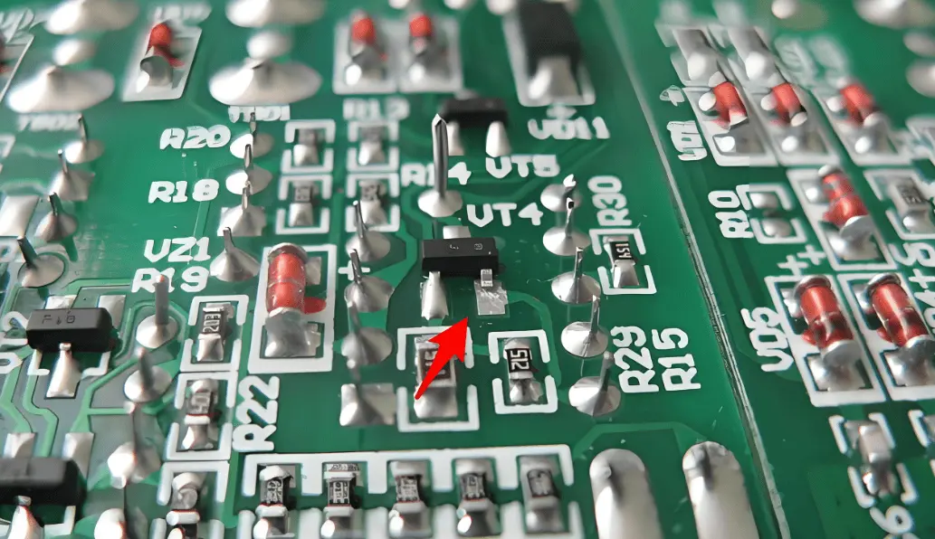
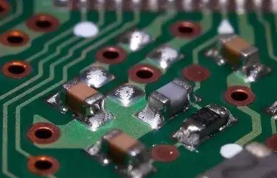
The principle of VI/EVI is based on the visual characteristics of cold solder joints, which differ from those of acceptable joints. Acceptable solder joints are smooth, shiny, and have a concave fillet that wraps uniformly around the component lead and PCB pad. Cold solder joints, by contrast, are dull, grainy, or frosty in appearance, with irregular or convex fillets, and may exhibit visible cracks, porosity, or incomplete wetting (e.g., "skipped" areas where solder does not adhere to the pad).
Equipment for EVI includes:Digital Microscopes: Offer magnification ranges from 20x to 200x, with high-resolution cameras for capturing detailed images of solder joints. Many models include adjustable LED illumination (coaxial, oblique, or ring lights) to highlight surface irregularities.Stereomicroscopes: Provide 3D visualization of solder joints, enabling inspection of fillet shape and wetting around component leads. Useful for inspecting through-hole components and surface-mount devices (SMDs) with complex geometries.Automated Optical Inspection (AOI) Systems: Automated EVI tools that use high-speed cameras and image analysis algorithms to compare solder joints against a reference standard. Advanced AOI systems can detect subtle defects such as dullness, porosity, and fillet irregularities associated with cold solder joints.
2.2 Operational Procedures
A systematic VI/EVI process for cold solder joint detection involves the following steps: Pre-Inspection Preparation: Clean the PCBA with isopropyl alcohol (IPA) to remove flux residues, dust, or oil, which can obscure solder joint defects. Handle the PCBA with lint-free gloves to prevent contamination.Targeted Inspection: Focus on components associated with the intermittent fault (e.g., components in the signal path where the fault occurs). For each component, inspect all solder joints for: Surface appearance (dullness, graininess, or frostiness).Fillet shape (irregular, convex, or incomplete).Visible cracks, porosity, or gaps between solder and pad/lead.Solder coverage (complete wetting of pad and lead).Comparison with Reference Standards: Use IPC-A-610 images or acceptable solder joints on the same PCBA as references to distinguish between cold solder joints and normal variations.Documentation: Capture images of suspected cold solder joints for later verification and troubleshooting.
2.3 Applicability and Limitations
VI/EVI is ideal for initial screening of SMDs (0402, 0603, QFP, SOIC) and through-hole components. It is fast, low-cost, and requires minimal equipment, making it suitable for both laboratory and production line environments. AOI systems, in particular, are effective for high-volume PCBA inspection, as they can process hundreds of solder joints per minute.
However, VI/EVI has significant limitations: Limited to Visible Joints: Cannot inspect hidden solder joints, such as those under BGA, CSP, or QFN packages, or joints covered by conformal coatings.Subjectivity: Manual VI relies on operator expertise; subtle cold solder joints may be misclassified as acceptable. While AOI reduces subjectivity, it may generate false positives for joints with normal surface variations.Inability to Detect Internal Defects: Cannot identify internal cracks, porosity, or poor intermetallic compound (IMC) formation, which are common in cold solder joints and contribute to intermittent faults.
3. X-Ray Inspection (2D and 3D)
X-ray inspection is a powerful NDT method that uses penetrating X-ray radiation to visualize hidden solder joints, making it ideal for detecting cold solder joints under BGA, CSP, QFN, and other area-array packages. It can also reveal internal defects (e.g., voids, cracks, incomplete wetting) that are invisible to visual inspection.
3.1 Principles and Equipment
X-ray inspection works based on the difference in X-ray absorption between materials. Solder (a high-density metal) absorbs more X-rays than the PCB substrate (low-density dielectric) or component packaging (plastic or ceramic), creating a contrast image that highlights the solder joint’s internal structure. Cold solder joints, with their porous, non-uniform structure and poor wetting, appear distinctively in X-ray images: Voids or porosity (dark spots) due to trapped gas during reflow.Incomplete wetting (lack of solder coverage on pads or BGA balls).Irregular solder joint shape (e.g., flat or misshapen BGA balls).Cracks (dark lines) in the solder joint.
Equipment for X-ray inspection includes: 2D X-Ray Systems: Generate 2D projection images of the PCBA. Suitable for basic inspection of hidden joints, such as detecting missing solder or large voids. Operate at low X-ray energies (10–40 kV) to avoid damaging components.3D X-Ray Computed Tomography (CT): Capture multiple 2D X-ray images from different angles and reconstruct them into a 3D model of the solder joint. Enables detailed analysis of internal structure, including void distribution, wetting depth, and IMC formation. High-end 3D X-ray systems offer sub-micron resolution, making them suitable for fine-pitch components (e.g., micro-BGA).
3.2 Operational Procedures
X-ray inspection for cold solder joint detection follows these steps: PCBA Positioning: Mount the PCBA on a motorized stage, ensuring that the area of interest (AOI) (e.g., BGA package associated with intermittent faults) is centered in the X-ray beam.Parameter Setup: Adjust X-ray voltage, current, and exposure time based on the PCBA’s thickness and component density. For 2D inspection, use a voltage of 20–30 kV for thin PCBs (1–2 layers) and 30–40 kV for thick multi-layer PCBs. For 3D CT, set the stage to rotate through 360° to capture multiple projections.Image Acquisition: Capture 2D images or 3D projection data. For 2D inspection, adjust the stage angle (tilt or rotate) to view the solder joint from different perspectives, enhancing defect visibility.Image Analysis: Use image processing software to enhance contrast, measure void size and distribution, and evaluate solder wetting. Compare the results against IPC standards (e.g., IPC-A-610 allows a maximum void area of 25% for BGA joints).Defect Classification: Classify defects as cold solder joints if they exhibit characteristic features (e.g., voids >25%, incomplete wetting, irregular shape) and correlate with the intermittent fault location.
3.3 Applicability and Limitations
X-ray inspection is the gold standard for inspecting hidden solder joints, making it indispensable for BGA, CSP, and QFN packages. It can detect internal defects that cause intermittent faults, such as small cracks or voids that disrupt electrical contact under stress. 3D X-ray CT, in particular, provides a comprehensive view of the solder joint’s structure, enabling precise defect characterization.
Limitations of X-ray inspection include: High Cost: X-ray systems are expensive (ranging from $50,000 to $500,000), making them impractical for small-scale operations.Operator Expertise Required: Interpreting X-ray images requires specialized training, as distinguishing between minor voids (acceptable) and cold solder joints (unacceptable) can be challenging.Potential Component Damage: While low-energy X-rays are safe for most components, prolonged exposure can damage sensitive devices (e.g., image sensors, organic semiconductors).Limited to High-Density Defects: X-ray inspection is less effective for detecting surface defects (e.g., dullness, surface cracks) on exposed solder joints, which are better detected by VI/EVI.
4. Thermal Cycling Testing Combined with Electrical Monitoring
Intermittent faults caused by cold solder joints are often triggered by thermal stress, as temperature changes induce thermal expansion/contraction of the PCB, components, and solder joints. Thermal cycling testing combined with real-time electrical monitoring simulates these stress conditions, forcing the cold solder joint to manifest as a measurable electrical fault (e.g., open circuit, increased resistance).
4.1 Principles and Equipment
The principle of this method is to subject the PCBA to controlled temperature cycles while monitoring the electrical continuity or resistance of the circuit associated with the intermittent fault. Cold solder joints, with their weak mechanical structure, will experience contact loss or resistance spikes when the solder joint expands or contracts beyond its brittle limit. By correlating temperature changes with electrical faults, engineers can confirm the presence of cold solder joints and locate their position.
Equipment required includes: Thermal Chamber: A controlled environment chamber capable of cycling temperatures between -55°C and 150°C (or wider ranges for aerospace applications) with precise temperature control (±1°C). The chamber should have ports for electrical connections to monitor the PCBA during testing.Electrical Monitoring Equipment: Devices to measure continuity, resistance, or voltage in real time, such as: Digital multimeters (DMMs) with data logging capabilities.Oscilloscopes for monitoring high-frequency signals.In-Circuit Test (ICT) systems or Functional Test (FT) fixtures for comprehensive circuit monitoring.Thermocouples: To measure the actual temperature of the PCBA (not just the chamber temperature) and correlate it with electrical faults.
4.2 Operational Procedures
Thermal cycling testing with electrical monitoring involves the following steps: Test Setup: Connect the PCBA to the electrical monitoring equipment (DMM, oscilloscope, or FT fixture) and route the cables through the thermal chamber’s ports.Attach thermocouples to the PCBA near the components associated with the intermittent fault (e.g., BGA, connector) to monitor local temperature.Program the thermal chamber with temperature cycles that simulate the PCBA’s end-use environment. A typical cycle includes: Ramp-up from ambient to high temperature (e.g., 125°C) at 5°C/min.Dwell at high temperature for 30 minutes.Ramp-down to low temperature (e.g., -40°C) at 5°C/min.Dwell at low temperature for 30 minutes.Repeat the cycle 10–100 times (depending on the application’s reliability requirements).Real-Time Monitoring: Start the thermal chamber and electrical monitoring equipment. Log data continuously, including temperature, resistance, continuity, or signal integrity. Set alarms to trigger when electrical faults (e.g., resistance >1Ω, loss of continuity) occur.Fault Correlation: Analyze the logged data to determine if faults occur during specific phases of the thermal cycle (e.g., ramp-up, ramp-down, or dwell). Faults that coincide with temperature changes strongly indicate cold solder joints.Defect Localization: If the fault is detected, use additional testing (e.g., X-ray, VI/EVI) to inspect the solder joints of the components in the fault circuit.
4.3 Applicability and Limitations
This method is highly effective for verifying that intermittent faults are caused by cold solder joints, as it directly simulates the environmental stress that triggers the fault. It is particularly useful for high-reliability applications (aerospace, automotive, medical) where intermittent faults under extreme temperatures are unacceptable.
Limitations include: Long Test Duration: Thermal cycling tests can take hours or days to complete (e.g., 100 cycles × 2 hours per cycle = 200 hours), making them impractical for fast-paced production environments.Equipment Cost: Thermal chambers and high-precision monitoring equipment are expensive, requiring significant capital investment.Limited Defect Localization: The method indicates that a fault exists in a specific circuit but does not directly identify the exact solder joint. Additional testing (e.g., X-ray) is required for precise localization.
5. Vibration Testing Combined with Electrical Monitoring
Like thermal stress, mechanical vibration can trigger intermittent faults in cold solder joints by causing the weak joint to lose contact temporarily. Vibration testing combined with electrical monitoring simulates the mechanical stress encountered during transportation, installation, or end-use (e.g., automotive, industrial machinery) and detects faults caused by cold solder joints.
5.1 Principles and Equipment
The principle is similar to thermal cycling testing: the PCBA is subjected to controlled vibration while monitoring electrical continuity or signal integrity. Cold solder joints, with their poor mechanical adhesion, will experience contact loss or resistance spikes when vibrated, as the solder joint shifts or cracks under mechanical stress. By correlating vibration parameters (frequency, amplitude) with electrical faults, engineers can confirm the presence of cold solder joints.
Equipment required includes: Vibration Shaker System: A shaker table capable of generating sinusoidal, random, or transient vibration in the frequency range of 10–2000 Hz (or higher for specialized applications). The system should have a fixture to mount the PCBA securely while allowing electrical connections.Electrical Monitoring Equipment: Same as thermal cycling testing (DMMs, oscilloscopes, ICT/FT systems) for real-time data logging of continuity, resistance, or signal integrity.Accelerometers: To measure the actual vibration amplitude and frequency at the PCBA level, ensuring that the test conditions match the end-use environment.
5.2 Operational Procedures
Vibration testing with electrical monitoring follows these steps: Test Setup: Mount the PCBA on the vibration shaker using a fixture that mimics its actual mounting in the end product (e.g., screws, adhesive). This ensures that the vibration is transmitted to the solder joints realistically.Connect the PCBA to the electrical monitoring equipment and route the cables to avoid interference with the vibration.Attach accelerometers to the PCBA near the fault-prone components to measure vibration levels.Program the vibration shaker with parameters that simulate the end-use environment:Sinusoidal Vibration: Sweep frequency from 10–2000 Hz at a constant amplitude (e.g., 1g) for 10–30 minutes.Random Vibration: Apply a power spectral density (PSD) profile (e.g., 0.01g²/Hz from 10–2000 Hz) for 10–30 minutes, simulating real-world vibration (e.g., automotive road noise).Real-Time Monitoring: Start the vibration shaker and electrical monitoring equipment. Log data continuously, setting alarms for electrical faults (e.g., loss of continuity, signal distortion).Fault Correlation: Analyze the data to determine if faults occur at specific frequencies or amplitudes. Cold solder joints often exhibit faults at resonance frequencies, where the PCBA or component vibrates most intensely.Defect Localization: Use additional testing (e.g., X-ray, VI/EVI) to inspect the solder joints in the fault circuit.
5.3 Applicability and Limitations
This method is ideal for detecting cold solder joints in PCBs used in vibration-prone environments (automotive, aerospace, industrial machinery). It is more rapid than thermal cycling testing (typical test duration: 30 minutes–2 hours) and can be integrated into production line quality control for high-reliability products.
Limitations include: Equipment Cost: Vibration shaker systems are expensive, especially for high-frequency or high-amplitude applications.Fixture Design Criticality: Poor fixture design can cause the PCBA to vibrate unevenly, leading to false results. The fixture must replicate the actual mounting conditions accurately.Limited Defect Localization: Like thermal cycling testing, it indicates a fault in a circuit but not the exact solder joint.
6. Electrical Test Methods: ICT, FT, and JTAG
Electrical test methods, such as In-Circuit Test (ICT), Functional Test (FT), and JTAG (Joint Test Action Group) testing, focus on the electrical performance of the PCBA to detect faults caused by cold solder joints. These methods are particularly effective for identifying intermittent faults that affect circuit continuity or signal integrity.
6.1 In-Circuit Test (ICT)
ICT uses a bed-of-nails fixture to make electrical contact with test points on the PCBA, measuring the resistance, capacitance, and inductance of individual components and traces. Cold solder joints cause increased resistance or intermittent open circuits, which are detected by comparing the measured values against nominal specifications.
Advantages: Highly accurate for detecting continuity issues in specific components or traces.Fast test speed (suitable for high-volume production).Can localize faults to specific components or solder joints.
Limitations: Requires custom test fixtures, which are expensive for low-volume or prototype PCBs.Cannot test components without test points (e.g., BGA packages with no exposed leads).May not detect intermittent faults that only appear under stress (thermal, vibration).
6.2 Functional Test (FT)
FT tests the PCBA’s overall functionality by simulating end-use operating conditions (e.g., applying input signals, measuring output responses). Intermittent faults caused by cold solder joints will manifest as incorrect output signals, system crashes, or performance degradation.
Advantages: Tests the PCBA as a complete system, detecting faults that affect real-world performance.No need for custom fixtures (for basic FT); can use standard test equipment (oscilloscopes, signal generators).Can be combined with thermal or vibration testing to detect stress-induced intermittent faults.
Limitations: Limited fault localization (indicates a system-level fault but not the exact solder joint).Test development time is long for complex PCBs.May not detect subtle cold solder joints that do not affect overall functionality under static conditions.
6.3 JTAG Testing
JTAG (IEEE 1149.1) is a standard for testing and debugging digital circuits. It uses dedicated test pins (TCK, TMS, TDI, TDO) to access internal registers of components (e.g., microcontrollers, FPGAs, CPLDs). Cold solder joints in the JTAG chain or in the component’s power/ground connections will cause communication errors or test failures.
Advantages: No need for custom fixtures (uses standard JTAG test points).Can test internal components and interconnections, including those in BGA or QFP packages.Fast and efficient for digital circuit testing.
Limitations: Only applicable to digital components that support JTAG.Cannot test analog circuits or passive components.May not detect cold solder joints in non-JTAG-related circuits.
7. Acoustic Microscopy (SAM)
Scanning Acoustic Microscopy (SAM) uses high-frequency ultrasound waves (10–200 MHz) to inspect the internal structure of solder joints. It is particularly effective for detecting delamination, cracks, and voids in solder joints—key characteristics of cold solder joints.
7.1 Principles and Equipment
SAM works by transmitting ultrasound waves through the PCBA. When the waves encounter a boundary between materials with different acoustic impedances (e.g., solder and PCB substrate, solder and component lead), they reflect back to a transducer. Cold solder joints, with their porous structure or poor adhesion, have different acoustic impedance properties than acceptable joints, resulting in distinct reflection patterns. SAM can generate 2D or 3D images of the solder joint’s internal structure, highlighting defects such as voids, cracks, and delamination.
Equipment: Scanning acoustic microscopes with high-frequency transducers (50–150 MHz) for detailed inspection of solder joints. Advanced systems offer phase contrast and amplitude imaging to enhance defect visibility.
7.2 Operational Procedures
SAM inspection for cold solder joints involves: PCBA Preparation: Immerse the PCBA in a coupling fluid (e.g., deionized water, glycerol) to transmit ultrasound waves (air absorbs ultrasound, so a coupling medium is required).Transducer Setup: Select a transducer frequency based on the solder joint size (higher frequency for smaller joints). Set the scan area to cover the components associated with the intermittent fault.Image Acquisition: Scan the PCBA, capturing reflection data from the solder joints. Adjust the focal plane to focus on the solder joint (between the PCB pad and component lead).Image Analysis: Analyze the acoustic images to identify defects. Cold solder joints appear as bright or dark areas (depending on the defect type) due to irregular reflection of ultrasound waves. Voids and cracks appear as dark spots or lines, while delamination appears as a bright boundary.
7.3 Applicability and Limitations
SAM is highly effective for detecting internal defects in solder joints, including those under BGA, QFN, and other hidden packages. It can identify defects that are not visible with X-ray inspection (e.g., delamination between solder and pad). SAM is also non-damaging and can be used for both prototype and production PCBs.
Limitations: High Cost: SAM systems are expensive, similar to X-ray systems.Coupling Fluid Requirement: The PCBA must be immersed in a coupling fluid, which requires additional cleaning after testing. This is not suitable for PCBs with sensitive components (e.g., connectors, sensors) that cannot be exposed to fluid.Limited to Thin PCBs: High-frequency ultrasound waves are attenuated by thick PCBs or metal shields, limiting inspection depth.
8. Selection of Non-Destructive Testing Methods for Intermittent Faults Suspected of Cold Solder Joints
The selection of the appropriate NDT method depends on several factors, including the PCBA’s design (component types, package sizes), the nature of the intermittent fault, the available equipment, and the application’s reliability requirements. A systematic approach to method selection is as follows:Initial Screening with VI/EVI or AOI: Use visual or enhanced visual inspection to check exposed solder joints for obvious cold solder joint characteristics (dullness, irregular fillets). This is a low-cost, fast first step.Test for Hidden Joints with X-Ray or SAM: If the fault is associated with hidden joints (BGA, QFN), use X-ray inspection (2D or 3D) or SAM to visualize internal defects.Simulate Stress Conditions with Thermal/Vibration Testing: If the intermittent fault is triggered by environmental stress, use thermal cycling or vibration testing combined with electrical monitoring to confirm that the fault is caused by cold solder joints.Localize Faults with Electrical Testing: Use ICT, FT, or JTAG to narrow down the fault to a specific circuit or component, then use X-ray or VI/EVI to inspect the solder joints in that area.
For high-reliability applications (aerospace, medical), a combination of methods is recommended (e.g., X-ray + thermal cycling + SAM) to ensure comprehensive defect detection.
9. Conclusion
Intermittent faults in PCBA functional testing suspected of being caused by cold solder joints are a significant quality challenge, as their erratic nature makes them difficult to diagnose. Non-destructive testing methods provide a reliable means of detecting these subtle defects without damaging the PCBA, ensuring that only high-quality assemblies reach the end user. Visual and enhanced visual inspection serve as effective initial screening tools for exposed solder joints, while X-ray and acoustic microscopy are indispensable for inspecting hidden joints and internal defects. Thermal cycling and vibration testing, combined with real-time electrical monitoring, simulate the environmental stress that triggers intermittent faults, confirming the presence of cold solder joints. Electrical test methods (ICT, FT, JTAG) aid in fault localization, narrowing down the defect to specific circuits or components.