 PCB
PCB FPC
FPC Rigid-Flex
 FR-4
FR-4 HDI PCB
 Rogers High-Frequency Board
 PTFE Teflon High-Frequency Board
 Aluminum
 Copper Core
 PCB Assembly
 LED light PCBA
 Memory PCBA
 Power Supply PCBA
 New Energey PCBA
 Communication PCBA
 Industrial Control PCBA
 Medical Equipment PCBA
 Testing Service
 PCBA Testing Service
 Certification Application
 RoHS Certification Application
 REACH Certification Application
 CE Certification Application
 FCC Certification Application
 CQC Certification Application
 UL Certification Application
 Transformers, Inductors
 High Frequency Transformers
 Low Frequency Transformers
 High Power Transformers
 Conversion Transformers
 Sealed Transformers
 Ring Transformers
 Inductors
 Wires,Cables Customized
 Network Cables
 Power Cords
 Antenna Cables
 Coaxial Cables
 Net Position Indicator
 Solar AIS net position indicator
 Capacitors
 Connectors
 Diodes
 Embedded Processors & Controllers
 Digital Signal Processors (DSP/DSC)
 Microcontrollers (MCU/MPU/SOC)
 Programmable Logic Device(CPLD/FPGA)
 Communication Modules/IoT
 Resistors
 Through Hole Resistors
 Resistor Networks, Arrays
 Potentiometers,Variable Resistors
 Aluminum Case,Porcelain Tube Resistance
 Current Sense Resistors,Shunt Resistors
 Switches
 Transistors
 Power Modules
 Isolated Power Modules
 AC-DC Power Modules
 DC-AC Module(Inverter)
 RF and Wireless
Calculation Method for Etch Compensation Factor in Outer Layer Traces
Calculation Method for Etch Compensation Factor in Outer Layer Traces
In PCB manufacturing, the etch compensation factor is critICal to ensure the final trace width meets design specifications. This factor accounts for material loss during etching, including both vertical and lateral removal (undercut). Below is a detailed explanation of its principles, calculation, and practical application.
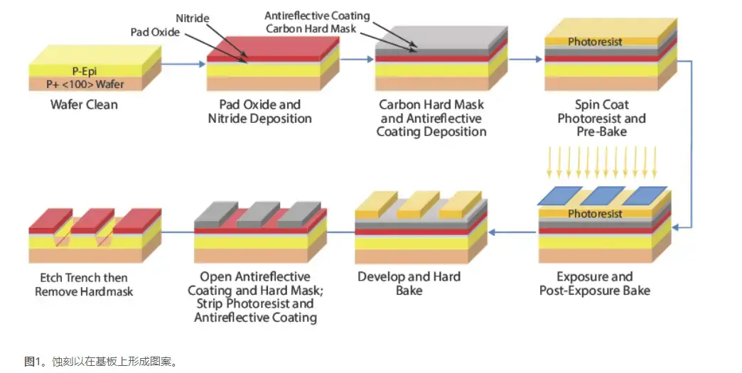
1. Fundamentals of Etch Compensation
The compensation factor adjusts the design dimensions to offset copper loss during etching. Key factors include:
-
Etch Factor (EF):
Defined as the ratio of vertical etch depth to undercut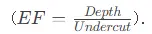
Higher EF reduces undercut, lowering compensation needs. -
Copper Thickness (T):
Standard thickness (e.g., 1 oz=35μm) directly affects etch time and undercut. -
Etchant and Process Parameters:
Acidic (e.g., FeCl₃) and alkaline (e.g., ammonia-based) etchants behave differently, requiring tailored adjustments.
2. Formula Derivation
-
Undercut Calculation:
Example: For 35μm copper (1 oz) and EF=3.0, .
-
Single-Side Compensation (ΔW):
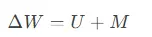
M is a safety margin (1-2μm) to account for process variability.
-
Total Compensation Factor (C):
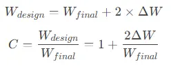

3. Practical Implementation Steps
-
Measure Etch Factor:
-
Use test coupons to determine undercut and vertical etch depth.
-
Calculate average EF.
-
-
Select Compensation Model:
-
Linear Compensation: For uniform etching (e.g., panel-wide).
-
Zone-Based Compensation: Adjust high-density areas separately.
-
-
Optimize Process Parameters:
-
Control etchant temperature (30-50℃), spray pressure (1.5-2.5 bar), and conveyor speed.
-
Monitor etch rate (μm/min) and dynamically adjust exposure patterns.
-
4. Case Study
Scenario:
A 6-layer PCB with 1 oz outer copper, target trace width 100μm, and measured EF=2.5.
Steps:
-
Undercut: .
-
Single-side compensation (): .
-
Design width: .
-
Compensation factor: .
Verification:
Post-etch measured width: 102μm (within ±10% tolerance).
5. Key Considerations
-
Material Variability:
Low-roughness copper (e.g., HVLP) reduces undercut, allowing lower compensation. -
Pattern Density:
Isolated traces require higher compensation than dense ones. -
Advanced Processes:
For mSAP (modified semi-additive process), integrate plating thickness into models.
6. Conclusion
Accurate etch compensation requires integrating EF, copper thickness, and process conditions, validated through iterative testing. Mastering this method enhances yield and consistency in high-frequency, high-density PCB manufacturing.