 PCB
PCB FPC
FPC Rigid-Flex
 FR-4
FR-4 HDI PCB
 Rogers High-Frequency Board
 PTFE Teflon High-Frequency Board
 Aluminum
 Copper Core
 PCB Assembly
 LED light PCBA
 Memory PCBA
 Power Supply PCBA
 New Energey PCBA
 Communication PCBA
 Industrial Control PCBA
 Medical Equipment PCBA
 Testing Service
 PCBA Testing Service
 Certification Application
 RoHS Certification Application
 REACH Certification Application
 CE Certification Application
 FCC Certification Application
 CQC Certification Application
 UL Certification Application
 Transformers, Inductors
 High Frequency Transformers
 Low Frequency Transformers
 High Power Transformers
 Conversion Transformers
 Sealed Transformers
 Ring Transformers
 Inductors
 Wires,Cables Customized
 Network Cables
 Power Cords
 Antenna Cables
 Coaxial Cables
 Net Position Indicator
 Solar AIS net position indicator
 Capacitors
 Connectors
 Diodes
 Embedded Processors & Controllers
 Digital Signal Processors (DSP/DSC)
 Microcontrollers (MCU/MPU/SOC)
 Programmable Logic Device(CPLD/FPGA)
 Communication Modules/IoT
 Resistors
 Through Hole Resistors
 Resistor Networks, Arrays
 Potentiometers,Variable Resistors
 Aluminum Case,Porcelain Tube Resistance
 Current Sense Resistors,Shunt Resistors
 Switches
 Transistors
 Power Modules
 Isolated Power Modules
 AC-DC Power Modules
 DC-AC Module(Inverter)
 RF and Wireless
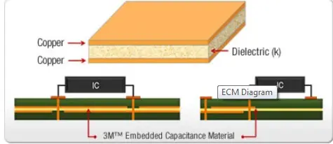
Controlling Capacitance Tolerance of Embedded Capacitors in Buried Passive Component Processes
1. Key Sources of Capacitance Deviation
Capacitance tolerance (typICally within ±10%) is influenced by:
-
Dielectric material variation: Batch-to-batch differences in Dk and thickness;
-
Process drift: Uneven lamination pressure/temperature, etching inaccuracies, copper foil roughness (Rz);
-
Design mismatch: Pad-dielectric misalignment, unaccounted fringing effects;
-
Environmental factors: Humidity sensitivity (e.g., FR-4 Dk shifts ~0.5%/RH%).
2. Core Control Strategies
(1) Material Selection and Pre-Treatment
-
Stable dielectrics:
-
Use low-Dk-tolerance materials (e.g., 3M C-Ply, DuPont Interra) with ±5% Dk consistency;
-
For high-frequency applications, select low-loss (Df<0.003) resins with stable TCC.
-
-
Pre-treatment:
-
Pre-bake dielectric films (120°C/2h) to remove moisture;
-
Roughen copper foil (Rz≤3μm) to improve adhesion.
-
(2) Process Optimization
-
Lamination control:
-
Use vacuum lamination with pressure profiling (0.5→3.0 MPa) and ±2°C temperature uniformity;
-
Monitor dielectric thickness via laser sensors (±1μm) for real-time feedback.
-
-
Pattern accuracy:
-
Apply LDI for ±5μm electrode linewidth control;
-
Post-etch AOI to ensure >85° sidewall angles.
-
(3) Design Compensation and SIMulation
-
Structure optimization:
-
Simulate fringing effects (e.g., ANSYS HFSS) and add overlap margins (≥50μm);
-
Use distributed Capacitor arrays to reduce sensitivity.
-
-
Impedance matching:
-
Adjust reference planes via TLM to minimize parasitic inductance.
-
(4) In-Line Monitoring and Feedback
-
Capacitance testing:
-
Embed LCR test points for fly-probing (1 MHz) at critical stages;
-
Apply SPC to track Cp/Cpk and adjust process windows.
-
-
Environmental control:
-
Maintain 40±5% RH and 23±1°C in cleanrooms.
-
3. Tolerance Compensation Techniques
-
Laser trimming:
-
Adjust electrode area via laser ablation (±1% accuracy);
-
Ideal for high-frequency/mmWave applications.
-
-
Programmable capacitor arrays:
-
Use binary-weighted units with fuses/switches to compensate ±15% initial deviation.
-
4. Failure Analysis and Process Improvement
-
Root cause analysis:
-
Perform cross-sectioning and SEM/EDS on failed capacitors to identify defects (delamination, voids);
-
Build defect libraries linking process parameters to deviations.
-
-
DOE optimization:
-
Apply Taguchi Method to identify critical factors (e.g., lamination temperature).
-
5. Challenges and Solutions
-
Challenge 1: Thin dielectric uniformity (<20μm)
-
Solution: Nano-scale coating (e.g., slot-die coating) with <±3% thickness variation.
-
-
Challenge 2: High-frequency stability
-
Solution: Low-TCC materials (e.g., polyimide composites, TCC<±50 ppm/°C).
-
-
Challenge 3: Mass production consistency
-
Solution: AI-driven adaptive systems for real-time parameter compensation.
-