 PCB
PCB FPC
FPC Rigid-Flex
 FR-4
FR-4 HDI PCB
 Rogers High-Frequency Board
 PTFE Teflon High-Frequency Board
 Aluminum
 Copper Core
 PCB Assembly
 LED light PCBA
 Memory PCBA
 Power Supply PCBA
 New Energey PCBA
 Communication PCBA
 Industrial Control PCBA
 Medical Equipment PCBA
 Testing Service
 PCBA Testing Service
 Certification Application
 RoHS Certification Application
 REACH Certification Application
 CE Certification Application
 FCC Certification Application
 CQC Certification Application
 UL Certification Application
 Transformers, Inductors
 High Frequency Transformers
 Low Frequency Transformers
 High Power Transformers
 Conversion Transformers
 Sealed Transformers
 Ring Transformers
 Inductors
 Wires,Cables Customized
 Network Cables
 Power Cords
 Antenna Cables
 Coaxial Cables
 Net Position Indicator
 Solar AIS net position indicator
 Capacitors
 Connectors
 Diodes
 Embedded Processors & Controllers
 Digital Signal Processors (DSP/DSC)
 Microcontrollers (MCU/MPU/SOC)
 Programmable Logic Device(CPLD/FPGA)
 Communication Modules/IoT
 Resistors
 Through Hole Resistors
 Resistor Networks, Arrays
 Potentiometers,Variable Resistors
 Aluminum Case,Porcelain Tube Resistance
 Current Sense Resistors,Shunt Resistors
 Switches
 Transistors
 Power Modules
 Isolated Power Modules
 AC-DC Power Modules
 DC-AC Module(Inverter)
 RF and Wireless
Effective Removal of Residual Copper Debris from Board Edges After Routing and V-Cut Without Surface Damage
2026-02-01
In the manufacturing process of printed Circuit Boards (PCBs), mechanical profiling operations represented byrouting (milling)and V‑cutting serve as critical procedures to separate single boards from a panel and form the final product outline. Nevertheless, these mechanical processes inevitably produce fine copper particles, burrs and resin fiber residues, which tend to adhere to board edges, internal grooves and suRFace metallization structures.Residual copper debris not only causes appearance defects but also brings about severe reliability risks including electrical short circuits, decreased surface insulation resistance and electrochemical migration during service. Meanwhile, improper cleaning strategies tend to induce secondary quality defects, such as solder mask scratching and peeling, pad discoloration, substrate delamination and fine circuit deformation.
Targeting the core engineering issue—how to effectively remove residual copper debris from board edges after routing and V‑cut without damaging the PCB surface—this paper systematically expounds the formation mechanism and distribution traits of copper residues, categorizes and evaluates mainstream cleaning technologies, proposes a stepwise integrated cleaning flow, establishes matched quality inspection criteria, and summarizes on‑site process optimization and preventive control strategies. With detailed technical parameters, comparative analysis and standardized application guides, the article provides practical and replicable solutions for PCB manufacturers to strengthen cleaning efficiency, guarantee product reliability and reduce post‑profiling quality defects.
1. Introduction
1.1 Background and Significance
Mechanical profiling is widely applied in the production of rigid and rigid‑flex PCBs. Routing adopts high‑speed rotating milling cutters to contour complex board shapes, while V‑cutting forms symmetrical V‑shaped grooves along preset dividing lines to facilitate subsequent splitting. Both operations involve direct mechanical interaction between cutting tools and copper‑clad laminates (CCL), leading to the synchronous generation of metallic and non‑metallic residues. Among these residues, residual copper debris features high conductivity and is prone to bridging adjacent circuits, becoming one of the primary triggers for electrical testing failures and in‑service functional breakdowns.
Driven by the rapid evolution of 5G communication, automotive electronics, consumer electronics and high‑end industrial control equipment, PCBs are developing toward high‑density interconnect (HDI), fine line width/spacing and multi‑layer stacking. In such advanced products, the tolerance for microscale contamination is extremely strict, and even tiny copper particles may result in catastrophic functional failures. Therefore, realizing thorough elimination of residual copper debris while safeguarding the structural integrity of solder masks, copper pads, plated through‑holes (PTHs) and surface finishes becomes essential to meet the acceptability requirements specified in IPC‑A‑600 and IPC‑6012.
1.2 Challenges in Cleaning Residual Copper Debris
The cleaning of residual copper debris after routing and V‑cut is restricted by multiple technical constraints, which increase the difficulty of balancing cleaning effectiveness and surface protection:
- Complex Adhesion States: Copper particles may embed into microcracks on board edges, attach to the concave‑convex surface of solder masks or get trapped in deep V‑grooves, making complete removal difficult with a single cleaning method.
- Material Sensitivity Differences: Modern PCB substrates (such as high‑frequency materials and thin‑core laminates) and surface finishing layers (including ENIG, ImAg, ENEPIG and HASL) possess distinct chemical stability and mechanical resistance, which limit the optional range of cleaning media and operating parameters.
- Risk of Secondary Surface Damage: Improper application of high‑pressure water jets, abrasive brushing tools or strong chemical cleaners may cause solder mask blistering, copper pad erosion, substrate swelling and fine line deformation.
- Matching of Production Efficiency: The cleaning process must match the operating tempo of profiling and subsequent assembly lines, requiring high continuous operation efficiency and good compatibility with automated mass production.
1.3 Scope and Structure of This Article
This article focuses on rigid PCBs after routing and V‑cut profiling, covering the characterization of residual copper debris, analysis of cleaning mechanisms, selection of technical routes, design of integrated processes, formulation of inspection standards and process optimization strategies. All technical content complies with mainstream IPC industry specifications and is applicable to actual mass production scenarios.
2. Formation Mechanism and Characteristics of Residual Copper Debris After Routing and V-Cut
2.1 Material Removal Mechanism in Mechanical Profiling
2.1.1 Routing (Milling) Process
Routing uses solid carbide end mills rotating at 10,000–60,000 rpm to perform peripheral cutting and plunge cutting. The cutter shears and fractures copper foil and dielectric base materials simultaneously. Under high‑speed cutting conditions, ductile copper foil undergoes intensive plastic deformation before fracture, forming flaky and granular residual copper debris, while brittle epoxy resin and glass fiber cloth produce dust and fibrous impurities. Part of the debris is discharged through the chip removal groove of the cutter, and the rest is pressed onto the board surface and edge under axial force, forming stable adhesion.
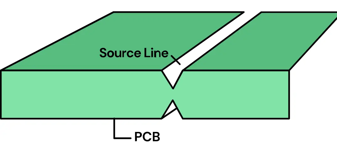
2.1.2 V-Cutting Process
V‑cutting employs a pair of oppositely arranged rotating circular blades to extrude and shear the board, forming a V‑shaped groove with controllable residual thickness (commonly 0.1–0.5 mm). The combined action of extrusion and shearing produces slender copper slivers and burrs along the groove edge, creates microvoids and rough surfaces that are prone to trapping micro copper particles, and may cause slight warping of the edge copper foil, further enhancing the adhesion strength of residual copper debris.
2.2 Morphology and Classification of Residual Copper Debris
Combined with industrial actual observation and metallographic microscope analysis, residual copper debris after mechanical profiling can be divided into three categories according to particle size and distribution state:
- Macro Copper Burrs: Linear or flaky copper protrusions with a size larger than 50 μm, which can be identified by naked eyes, mainly distributed along linear routing edges and V‑cut groove walls. Such debris mostly originates from incomplete shearing of copper foil caused by dull cutting tools or insufficient cutting force.
- Micro Copper Particles: Spherical or irregular particles with a size ranging from 5 μm to 50 μm, randomly dispersed on board edges and adjacent circuit surfaces. These particles are generated by high‑speed impact fracture and mild oxidation during the cutting process.
- Embedded Micro-debris: Particles smaller than 5 μm embedded in substrate microcracks, solder mask pinholes or PTH inner wall irregularities. This type of residual copper debris is the most difficult to remove and poses the highest reliability risk for fine‑pitch circuits.
2.3 Key Factors Affecting the Generation and Adhesion of Residual Copper Debris
2.3.1 Cutting Tool Condition
Tool sharpness is a core factor affecting the output of residual copper debris. Worn, notched or chipped cutters and blades will intensify the plastic deformation of copper, increasing the generation of burrs and embedded particles. Tools coated with titanium nitride (TiN) or diamond‑like carbon (DLC) can reduce friction coefficient and copper adhesion, effectively lowering the total amount of residues.
2.3.2 Process Parameter Setting
Mismatched spindle speed and feed rate will increase cutting heat and material smearing phenomenon, promoting the adhesion of residual copper debris to the board surface. Unstable cutting depth and unqualified V‑cut residual thickness will aggravate local stress concentration and material fragmentation. Inadequate cooling and lubrication conditions will lead to thermal softening of copper, making particles more likely to adhere to the board surface.
2.3.3 Base Material and Surface Coating Properties
High‑ductility electrolytic copper foil tends to form more flaky burrs than rolled copper foil. High‑Tg and halogen‑free substrates with high toughness usually produce more fiber impurities, which are easy to wrap and retain residual copper debris. The rough surface structure of solder masks provides more physical anchoring points for micro particles, enhancing the difficulty of cleaning.
2.4 Potential Risks Caused by Residual Copper Debris
Untreated residual copper debris will bring multiple potential risks to PCB performance and service life:
- Electrical Short Circuits: Conductive copper particles form bridges between adjacent traces or pads, directly leading to electrical testing failure.
- Electrochemical Migration (ECM): Under the combined action of humidity and bias voltage, copper ions migrate and separate out dendritic structures, inducing delayed short‑circuit failures.
- Decline in Surface Insulation Resistance (SIR): Residues reduce the surface insulation performance of the board, threatening long‑term reliability.
- Defects of Protective Coating: Residual copper debris interferes with the adhesion of conformal coatings, forming coating voids and weak bonding areas.
- Obstacles to Assembly Process: Particles may fall off during SMT placement and reflow, causing solder ball defects or component offset.
3. Classification and Technical Evaluation of Cleaning Methods for Residual Copper Debris
To balance the removal efficiency of residual copper debris and surface protection performance, current mainstream cleaning technologies are divided into mechanical cleaning, wet chemical cleaning, dry cleaning and composite cleaning systems. Each technical route has unique acting mechanisms, applicable scenarios, advantages and restrictive conditions.
3.1 Mechanical Cleaning Technologies
Mechanical cleaning removes residual copper debris through physical contact, fluid shear force or ultrasonic cavitation, and is mostly used as the primary procedure for bulk residue removal.
3.1.1 High-Pressure Water Jet Cleaning
This method uses high‑pressure deionized (DI) water jets to generate strong shear force, detaching surface and edge‑adhered residual copper debris. The typical process parameters are: pressure 2.0–8.0 bar, temperature 30–50 °C, matching fan‑shaped nozzles with a spray angle of 60°–90°. It has the advantages of environmental friendliness, high efficiency in removing macro debris and good compatibility with most PCB materials. However, excessively high pressure may cause solder mask warping or substrate delamination, and it is ineffective for deeply embedded particles. For surface protection, direct vertical jet impact on thin flexible areas, PTH openings and weakly bonded solder mask edges should be avoided.
3.1.2 Rotary Brush Cleaning
Rotary brushes with soft or medium hardness remove adhered residual copper debris through rotating sweeping. Common brush materials include nylon, polypropylene and conductive bristles, with a monofilament diameter of 0.1–0.3 mm. This method performs well in removing edge burrs and surface adsorbed particles, and the contact pressure can be adjusted flexibly. Abrasive brushes may scratch solder masks and soft surface finishes, and worn brushes are likely to re‑deposit contaminants. For sensitive surface finishes, non‑woven ultra‑fine fiber brushes should be selected, and stable contact pressure should be maintained.
3.1.3 Ultrasonic Cleaning
Ultrasonic waves with a frequency of 20–80 kHz induce cavitation effect in aqueous solution, generating micro jets that break the bonding force between residual copper debris and the board surface. It has excellent removal effect on micro particles and residues in complex structures such as V‑grooves and inner grooves. Nevertheless, improper use may cause microcracks in thin substrates or delicate circuits, and may damage fragile components after mounting. Safe application principles include limiting the use to bare boards before component mounting, adopting a frequency above 40 kHz for HDI boards, and controlling the immersion time within 30–120 seconds.
3.1.4 Air Knife Blow-Off
High‑velocity compressed air or nitrogen air curtain wipes off loose residual copper debris through momentum exchange. The process parameters are: air velocity 80–150 m/s, pressure 0.3–0.7 MPa, equipped with HEPA high‑efficiency filtration device. As a dry process, it has no chemical waste generation and is suitable for final drying and loose particle removal. It has weak effect on strongly adhered residues, and may disperse particles to clean areas without matched dust collection equipment.
3.2 Wet Chemical Cleaning Technologies
Wet chemical cleaning weakens the interface adhesion between residual copper debris and PCB surface through formulated cleaning agents, and is often combined with mechanical assistance to improve the removal effect.
3.2.1 Neutral / Mildly Alkaline Aqueous Cleaners
Such cleaners are composed of nonionic surfactants, chelating agents and organic additives, with a pH value of 7.0–9.5. Surfactants reduce surface tension and emulsify organic attachments, while chelating agents stabilize dissolved copper ions. It is suitable for all common surface finishes (ENIG, ImAg, HASL, OSP) and solder mask systems, with good safety performance. The recommended process parameters are: temperature 40–60 °C, immersion time 60–180 seconds, assisted by spray or ultrasonic vibration.
3.2.2 Weak Acid Cleaners
Weak acid cleaners are prepared from dilute organic acids (citric acid, acetic acid, gluconic acid), corrosion inhibitors and surfactants, with a pH value of 3.0–5.5. They mildly etch the surface of copper particles to break the oxide layer and reduce adhesion strength. They have a prominent effect on oxidized residual copper debris and must be equipped with efficient inhibitors to avoid etching copper pads. This type of cleaner is not recommended for OSP‑coated boards, and sufficient post‑cleaning rinsing is required to prevent acid residue retention.
3.2.3 Semi-Aqueous Cleaners
Semi‑aqueous cleaners adopt water‑miscible organic solvents (glycol ether) as the main component, matched with surfactants and builders. They have strong contaminant removal capacity and good compatibility with most laminate materials. The disadvantages include relatively high use cost and strict requirements for rinsing and waste liquid treatment.
3.3 Dry Cleaning Technologies
Dry cleaning avoids water‑based waste liquid and is suitable for moisture‑sensitive base materials and special surface finishes.
3.3.1 CO₂ Snow Cleaning
Liquid CO₂ is sprayed through a special nozzle to form solid CO₂ snow particles, which remove residual copper debris through momentum impact and sublimation cooling. The process is non‑abrasive, residue‑free and highly compatible with sensitive substrates and fine circuits. The disadvantages are high equipment investment and limited effect on heavily embedded residues.
3.3.2 Adhesive Roller Cleaning
Low‑viscosity polyurethane or silica gel adhesive rollers physically lift loose residual copper debris on the board surface through sticky contact. It features simple operation, low cost and complete dry process, and will not cause any surface damage. It is ineffective for embedded or strongly bonded particles, and the adhesive layer needs to be replaced regularly.
3.4 Comparative Evaluation of Cleaning Technologies
To facilitate the selection of cleaning routes for residual copper debris, key technologies are compared from multiple dimensions such as cleaning capacity, material compatibility, use cost and environmental impact, as shown in Table 1.
| Cleaning Method | Macro Debris | Micro Particles | Embedded Debris | Solder Mask Compatibility | Surface Finish Compatibility | Cost Level | Environmental Impact |
|---|---|---|---|---|---|---|---|
| High-Pressure Water Spray | High | Medium | Low | Moderate | Excellent | Low | Low |
| Rotary Soft Brush | High | High | Low | Good | Good | Low | Low |
| Ultrasonic Cleaning | Medium | High | Medium | Moderate | Excellent | Medium | Low |
| Neutral Aqueous Cleaning | Medium | High | Medium | Excellent | Excellent | Medium | Low |
| CO₂ Snow Cleaning | Medium | High | Medium | Excellent | Excellent | High | Very Low |
| Adhesive Roller | Medium | Low | None | Excellent | Excellent | Very Low | Very Low |
| Air Knife Blow-Off | Medium | Low | None | Excellent | Excellent | Low | Low |
3.5 Key Risks of Secondary Surface Damage
Improper parameter setting will lead to irreversible surface defects while cleaning residual copper debris:
- Solder Mask Damage: Peeling, blistering, scratching and discoloration caused by overhigh pressure, abrasive brushes or incompatible chemicals.
- Copper Pad Defects: Etching loss, surface discoloration and thickness reduction caused by aggressive cleaning agents or prolonged contact.
- Substrate Structure Defects: Delamination, swelling and microcracking induced by excessive mechanical stress or chemical corrosion.
- Fine Circuit Deformation: Plastic deformation of narrow lines caused by high‑pressure water jets or hard brushes.
4. Integrated Step-by-Step Cleaning Process Design for Residual Copper Debris
Based on the above technical analysis, an integrated multi‑stage cleaning process is designed to achieve thorough removal of residual copper debris with minimal surface damage risk. The process is divided into five sequential steps: pre‑cleaning assessment, bulk residue removal, refined deep cleaning, multi‑stage rinsing and neutralization, and controllable drying and inspection.
4.1 Stage 1: Pre-Cleaning Condition Assessment
Before formal cleaning, rapid on‑site evaluation is carried out to determine the targeted processing strategy for residual copper debris:
- Identify the type (burrs, particles, embedded impurities) and distribution area of residual copper debris.
- Confirm PCB substrate type, surface finish model, line width/spacing and special structural areas (thin plate areas, V‑grooves, inner holes).
- Check for pre‑existing defects such as solder mask voids and edge copper warping.
- Classify product sensitivity and adjust subsequent cleaning parameters accordingly.
4.2 Stage 2: Bulk Residual Copper Debris Removal
The core objective of this stage is to eliminate macro copper burrs and loose particles without applying excessive mechanical force. The recommended process sequence is: air knife blow‑off → low‑pressure water spray → soft adhesive roller cleaning.
Key parameters are set as follows: air knife pressure 0.4–0.6 MPa, adopting HEPA‑filtered dry compressed air, with an oblique incident angle of 30°–45°; water spray pressure 2.0–3.0 bar, water temperature 35–45 °C, using fan‑shaped nozzles with an overlapping rate of 10%–20%; adhesive roller selects medium viscosity, and the linear speed is synchronized with the conveyor speed. The protection focus is to avoid direct high‑pressure impact on the bottom of V‑grooves and thin substrate areas.
4.3 Stage 3: Refined Deep Cleaning
This stage aims to remove micro particles and weakly embedded residual copper debris through the synergistic effect of mechanical and chemical actions. Two configurable schemes are provided for products with different sensitivity levels.
4.3.1 Standard Route (General Rigid PCBs)
Adopt a spray cleaning machine equipped with an ultrasonic immersion zone, using a neutral weakly alkaline surfactant cleaning agent with a pH value of 8.0–9.0. Process parameters: spray zone pressure 3.0–5.0 bar, temperature 45–55 °C, processing time 60 seconds; ultrasonic zone frequency 40 kHz, temperature 45–50 °C, processing time 45–90 seconds. This route is applicable to PCBs with ENIG, ImAg, HASL surface finishes and standard FR‑4 substrates.
4.3.2 Sensitive Route (HDI / Thin-Core / High-Frequency Boards)
Adopt the combined process of CO₂ snow cleaning and soft rotary brush cleaning. CO₂ snow particle size is controlled at 50–200 μm, incident angle 45°–60°, scanning speed 200–500 mm/s; the brush uses ultra‑fine nylon bristles with minimal contact pressure. This scheme is suitable for OSP, ENEPIG surface finishes, thin‑core laminates and high‑frequency materials, effectively reducing the risk of surface damage while removing residual copper debris.
4.4 Stage 4: Multi-Stage Rinsing and Neutralization
The purpose of this stage is to completely remove chemical cleaning agents and avoid re‑deposition of dissolved impurities. The rinsing sequence is: tap water rinsing → primary DI water rinsing → final overflow DI water rinsing. Process parameters: rinsing temperature 30–40 °C, final rinsing water resistivity ≥ 15 MΩ·cm, total rinsing duration 60–120 seconds. For boards processed with weak acid cleaning agents, a weakly alkaline rinsing solution with a pH value of 7.5–8.5 is added to ensure the board surface returns to a neutral state.
4.5 Stage 5: Controllable Drying and Post-Cleaning Inspection
This stage realizes complete drying of the board and preliminary verification of the removal effect of residual copper debris, avoiding water spot defects and thermal damage. The combined system of hot air blow‑off and infrared (IR) drying is adopted, with hot air temperature controlled at 60–85 °C, and the conveyor speed adjusted to ensure thorough drying without overheating. After drying, preliminary visual inspection is carried out on board edges and V‑grooves to confirm that no obvious residual copper debris remains.
4.6 Process Layout and Compatibility Control
The integrated cleaning process is designed for an online layout to match the production tempo of routing and V‑cut equipment. Key layout principles: install a dust extraction system at the profiling and cleaning stations; set physical isolation between the dirty area and the clean area to prevent cross‑contamination; configure a real‑time parameter monitoring module to track spray pressure, temperature and rinsing water resistivity and maintain process stability.
5. Quality Inspection Standards and Verification Methods for Residual Copper Debris Removal
The cleaning effect of residual copper debris must be verified through standardized inspection methods in accordance with IPC‑A‑600G and IPC‑6012D specifications, and the integrity of the board surface structure must be confirmed simultaneously.
5.1 Visual Inspection Standards for Residual Copper Debris
5.1.1 Un-Aided Visual Inspection
Under 300–800 lux white light illumination, the acceptance standard is that no visible copper burrs, flakes or particle clusters can be observed on board edges, V‑grooves, inner holes and surrounding surfaces. This inspection is used for rapid screening of macro residual copper debris in mass production.
5.1.2 Microscopic Visual Inspection
Using a stereo optical microscope with a magnification of 10×–50×, the acceptance standard is that no discrete copper particles larger than 5 μm are present on key circuit surfaces, and no embedded residues exist in V‑grooves and PTH inner walls. This method is suitable for fine inspection of HDI boards and high‑reliability products.
5.2 Surface Structure Integrity Verification
5.2.1 Solder Mask Integrity Inspection
Check for scratching, blistering, peeling, pinholes and discoloration of the solder mask, and conduct a cross‑cut adhesion test in accordance with IPC‑TM‑650 2.4.28 to verify that the cleaning process of residual copper debris does not reduce the bonding strength of the solder mask.
5.2.2 Copper Pad State Inspection
Use X‑ray fluorescence (XRF) thickness measurement and metallographic section analysis to confirm that the copper pad has no etching loss, surface discoloration or structural damage.
5.2.3 Substrate Integrity Inspection
Microscopic observation confirms that the substrate has no delamination, swelling, fiber exposure and other defects, ensuring that the cleaning process does not damage the base material structure.
5.3 Reliability-Related Testing
For high‑reliability application scenarios such as automotive, industrial control and medical treatment, supplementary reliability testing is required on the basis of conventional inspection:
- Surface Insulation Resistance (SIR) Test: In accordance with IPC‑TM‑650 2.6.3.7, the minimum SIR value under high temperature and humidity conditions shall not be lower than 1×10⁸ Ω.
- Electrochemical Migration Test: In accordance with IPC‑TM‑650 2.6.16, no dendritic growth is allowed during biased humidity testing.
- Ionic Contamination Test: In accordance with IPC‑TM‑650 2.3.25, the total ionic contamination is controlled below 1.56 μg/cm² NaCl equivalent.
5.4 Sampling Plan and Inspection Frequency
Mass production adopts the AQL sampling plan specified in IPC‑STD‑001; key high‑reliability products implement 100% microscopic inspection on board edges and V‑groove areas; process stability audit selects representative samples to conduct SIR or ionic contamination testing weekly to monitor the long‑term stability of residual copper debris cleaning effect.
6. Process Optimization and Preventive Strategies for Residual Copper Debris Control
To reduce the generation of residual copper debris from the source and improve the stability of the cleaning process, targeted process optimization and preventive control measures are essential.
6.1 Profiling Process Parameter Optimization
6.1.1 Routing Parameter Tuning
Match spindle speed and feed rate according to substrate thickness and copper foil type: standard FR‑4 (1.0–1.6 mm) adopts 30,000–45,000 rpm and feed rate 80–150 mm/s; high‑Tg and thin substrates appropriately reduce the feed rate to reduce vibration and burr generation. Use sharp coated carbide cutters and establish a fixed tool replacement cycle (such as replacement after 10–20 machining hours). Adopt micro‑mist cooling and lubrication to reduce cutting heat and copper adhesion, thus reducing the output of residual copper debris.
6.1.2 V-Cut Parameter Optimization
Control the residual thickness within the tolerance range of ±0.05 mm of the set value; select precision grinding high‑speed steel or carbide V‑cut blades and maintain blade sharpness; optimize blade contact pressure to minimize edge copper warping and burr formation, reducing the adhesion amount of residual copper debris.
6.2 Fine-Tuning of the Cleaning Process
Establish classified parameter windows for different product grades to avoid over‑cleaning or insufficient cleaning of residual copper debris; configure a real‑time monitoring system for spray pressure, temperature and rinsing water resistivity; regularly maintain nozzles, brushes and filters to prevent re‑contamination; develop a quick‑switching cleaning formula library for different surface finishes and substrate types to improve flexible production capacity.
6.3 Equipment Maintenance and Management
Daily maintenance includes cleaning spray nozzles, checking brush wear status and replacing adhesive roller sheets; weekly calibration of pressure gauges, temperature sensors and ultrasonic generators; monthly inspection of conveyor system alignment, internal tank contamination detection and filter element replacement. Good equipment maintenance is an important guarantee for stable removal of residual copper debris.
6.4 Common Defect Troubleshooting
Table 2 summarizes typical defects related to residual copper debris cleaning, possible root causes and targeted corrective measures to guide on‑site rapid problem solving.
| Defect Description | Possible Root Causes | Corrective Actions |
|---|---|---|
| Residual copper particles remain | Insufficient cleaning power; clogged nozzles | Increase spray pressure/ultrasonic time; clean or replace nozzles |
| Solder mask scratching | Hard abrasive brushes; excessive contact pressure | Switch to soft fine-bristle brushes; reduce contact pressure |
| Water spots after drying | Inadequate rinsing; low DI water resistivity | Extend rinsing time; regenerate DI resin; optimize air knife layout |
| Pad discoloration (ENIG/ImAg) | Inappropriate chemical cleaner; prolonged exposure | Switch to neutral cleaner; reduce immersion time |
| V-groove residual debris | Ineffective spray coverage in narrow grooves | Use targeted small-angle nozzles; add ultrasonic cleaning |
7. Industrial Application Case Analysis
7.1 Case Background
An automotive PCB manufacturer produces double‑layer FR‑4 boards (thickness 1.6 mm, ENIG surface finish, line width/space 0.15 mm). After routing and V‑cut processes, the boards suffered from a high reject rate caused by residual copper debris, with an initial visual failure rate of about 8.5%, an SIR failure rate of about 3.2% and an ICT short‑circuit failure rate of about 2.1%, which seriously affected production efficiency and product delivery quality.
7.2 Implemented Solution
The manufacturer introduced the integrated cleaning process for residual copper debris proposed in this article: first, optimize the source control parameters, adjust the routing parameters to 40,000 rpm and 120 mm/s, establish a tool replacement cycle and add micro‑mist lubrication; second, upgrade the online cleaning line, adopting the process flow of air blow‑off → low‑pressure spray → ultrasonic‑assisted chemical cleaning → multi‑stage DI rinsing → hot air infrared drying; finally, improve the quality control system, implement 100% edge microscopic inspection and weekly SIR testing.
7.3 Outcome and Improvement Effect
After the implementation of the new process, the cleaning effect of residual copper debris was significantly improved: the visual defect rate dropped to less than 0.8%, the SIR failure was completely eliminated, the ICT short‑circuit failure rate was reduced to less than 0.3%, no solder mask or surface finish damage was found, and the overall production yield increased by about 7.2%. This case verifies the engineering feasibility and practical value of the integrated cleaning strategy in mass production.
8. Conclusion
Residual copper debris remaining on board edges after routing and V‑cut mechanical profiling is a key factor affecting PCB quality and reliability. Effective removal of such residues requires systematic understanding of the formation mechanism of residual copper debris, scientific selection and integrated matching of cleaning technologies, strict process parameter control and standardized effect verification.
This paper systematically analyzes the morphological characteristics and influencing factors of residual copper debris, evaluates the applicability of mainstream cleaning technologies, and constructs a multi‑stage integrated cleaning process that balances high removal efficiency and surface protection. Through the combination of profiling source control, physical‑chemical synergistic cleaning and reliable quality inspection, PCB manufacturers can significantly reduce contamination defects caused by residual copper debris and meet the strict application requirements of high‑end electronic products.
In the future, the development trend will focus on intelligent cleaning systems with real‑time residue detection and adaptive parameter adjustment, further improving the automation level, cleaning efficiency and process consistency of residual copper debris removal in multi‑variety and large‑batch production. All the technical schemes and operating guidelines proposed in this article comply with international industry standards and environmental protection regulations, providing a sustainable and reliable technical path for the control of residual copper debris in PCB manufacturing.