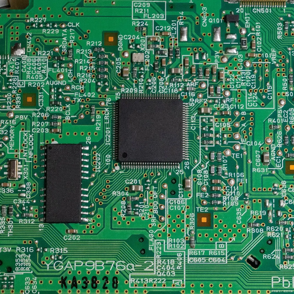
 PCB
PCB FPC
FPC Rigid-Flex
 FR-4
FR-4 HDI PCB
 Rogers High-Frequency Board
 PTFE Teflon High-Frequency Board
 Aluminum
 Copper Core
 PCB Assembly
 LED light PCBA
 Memory PCBA
 Power Supply PCBA
 New Energey PCBA
 Communication PCBA
 Industrial Control PCBA
 Medical Equipment PCBA
 Testing Service
 PCBA Testing Service
 Certification Application
 RoHS Certification Application
 REACH Certification Application
 CE Certification Application
 FCC Certification Application
 CQC Certification Application
 UL Certification Application
 Transformers, Inductors
 High Frequency Transformers
 Low Frequency Transformers
 High Power Transformers
 Conversion Transformers
 Sealed Transformers
 Ring Transformers
 Inductors
 Wires,Cables Customized
 Network Cables
 Power Cords
 Antenna Cables
 Coaxial Cables
 Net Position Indicator
 Solar AIS net position indicator
 Capacitors
 Connectors
 Diodes
 Embedded Processors & Controllers
 Digital Signal Processors (DSP/DSC)
 Microcontrollers (MCU/MPU/SOC)
 Programmable Logic Device(CPLD/FPGA)
 Communication Modules/IoT
 Resistors
 Through Hole Resistors
 Resistor Networks, Arrays
 Potentiometers,Variable Resistors
 Aluminum Case,Porcelain Tube Resistance
 Current Sense Resistors,Shunt Resistors
 Switches
 Transistors
 Power Modules
 Isolated Power Modules
 AC-DC Power Modules
 DC-AC Module(Inverter)
 RF and Wireless
 News Categories
Balancing Component Spacing and Heat Dissipation Path Requirements in High-Density PCB Layouts (Component Density > 100 components/in²)
2025-10-25
High-density PCBs (HDPCBs) with component densities exceeding 100 components per square inch are the backbone of modern miniaturized electronICs—from smartphones and wearables to aerospace sensors and AI accelerators. These designs pack hundreds to thousands of tiny components (e.g., 01005 chips, micro BGAs, and flip-chip ICs) into limited space, enabling smaller device footprints and higher functionality.
However, HDPCBs face a fundamental design conflict:
- Component spacing requirements: To avoid electrical inteRFerence (crosstalk), manufacturing defects (solder bridging), and rework accessibility, components need minimum spacing (typically 0.1–0.2mm for 01005 chips, 0.2–0.3mm for BGAs).
- Heat dissipation needs: High component density generates concentrated heat flux (often >10W/cm²), requiring unobstructed heat paths (e.g., thermal vias, copper pours, and airflow channels) to prevent component overheating (junction temperature >85℃ reduces reliability by 50% for most ICs).
Failing to balance these needs leads to two critical issues:
- Insufficient spacing: Causes short circuits, signal integrity degradation, or yield drops (from 95% to 70% in extreme cases).
- Blocked heat paths: Results in hotspots (>100℃), thermal throttling, or premature component failure.
Thus, HDPcb Layout requires a systematic approach to prioritize both spacing compliance and heat dissipation efficiency.
2. Foundational Principles for Balancing Spacing and Heat
Before diving into specific strategies, it is essential to establish two core principles that guide trade-off decisions:
2.1 Component Classification by Heat and Criticality
Not all components contribute equally to heat or require the same spacing. Classify components into four categories to prioritize resources:
- High-heat critical (HHC): High-power components (e.g., power management ICs, FPGAs) with >1W dissipation and safety-critical functions (e.g., processor cores). Require maximum heat path priority and moderate spacing flexibility.
- High-heat non-critical (HHN): High-power components (e.g., voltage regulators) with >1W dissipation but non-safety functions. Require heat path priority but more spacing flexibility.
- Low-heat critical (LHC): Low-power components (e.g., sensors, ADCs) with <0.1W dissipation but critical signal roles. Require strict spacing compliance and minimal heat path compromise.
- Low-heat non-critical (LHN): Low-power components (e.g., passives, LEDs) with <0.1W dissipation and non-critical functions. Offer the most flexibility for both spacing and heat path optimization.
2.2 Spacing Hierarchy (Based on IPC-2221 and IPC-7351)
Adopt a tiered spacing standard to ensure minimum electrical and manufacturing requirements are met, while allowing flexibility for heat paths:
- Tier 1 (Mandatory): Minimum spacing for electrical safety (e.g., 0.1mm between 01005 passives, 0.2mm between BGA pads). Violating this risks short circuits or solder bridging.
- Tier 2 (Recommended): Optimal spacing for manufacturing/rework (e.g., 0.15mm between 01005 passives, 0.25mm between BGAs). Provides margin for assembly variation.
- Tier 3 (Flexible): Extended spacing for heat/access (e.g., 0.2mm between 01005 passives) when space allows. Can be reduced to Tier 1 to accommodate heat paths for HHC components.
3. Layout Strategies to Balance Spacing and Heat Dissipation
The following strategies integrate spacing compliance with heat path design, tailored to HDPCB constraints:
3.1 Thermal-Aware Component Placement
Start placement by grouping components to minimize heat concentration while respecting spacing:
- Cluster HHC components: Place high-heat critical components (e.g., two 2W PMICs) near each other but with Tier 2 spacing (0.25mm) to create a centralized heat zone. This allows shared heat paths (e.g., a single large copper pour) instead of scattered paths that waste space.
- Separate HHC from LHC components: Maintain Tier 3 spacing (0.3mm) between HHC and LHC components (e.g., a processor and an ADC) to prevent thermal crosstalk (heat from HHC altering LHC signal accuracy) without sacrificing density.
- Stagger LHN components: Arrange low-heat non-critical components (e.g., 01005 resistors) in a staggered grid instead of a straight line. This reduces required spacing by 10–15% (from 0.15mm to 0.13mm) while maintaining airflow gaps for heat dissipation.
3.2 Compact Heat Path Integration Within Spacing Constraints
Traditional heat paths (wide copper pours, large thermal vias) are space-intensive—HDPCBs require miniaturized, targeted solutions:
- Micro Thermal Vias: Use 0.1–0.15mm diameter thermal vias (instead of 0.2mm standard vias) placed in the "dead space" between components (e.g., between BGA pads or 01005 passives). A 0.1mm via has a thermal resistance of ~50K/W (vs. 30K/W for 0.2mm) but occupies 75% less area. Cluster 4–6 micro vias under HHC components to achieve equivalent heat dissipation to a single standard via.
- Thermal Land Pads with Spacing Optimization: For BGAs, design thermal land pads (for heat dissipation) with spaced copper fingers (0.1mm wide, 0.1mm spacing) instead of solid pads. This maintains 80% of the thermal conductivity of a solid pad while allowing signal traces to pass through, reducing the need for extra spacing around the BGA.
- Buried Resistive Heatsinks: Integrate thin-film resistive heatsinks (NiCr, 1–2μm thick) directly on the PCB surface between high-heat components. These heatsinks occupy <0.05mm² per component and increase heat dissipation by 15–20% without requiring additional spacing.
3.3 Dynamic Spacing Adjustment for Heat Prioritization
Use the spacing hierarchy to adjust distances dynamically, prioritizing heat paths for HHC components:
- Relax LHN spacing for HHC heat paths: Reduce spacing between LHN components (e.g., from 0.15mm to 0.1mm, Tier 1) to create a 0.2mm-wide heat channel leading to a copper pour near an HHC component. This sacrifices non-critical spacing to enable critical heat dissipation.
- Implement "Heat Breaks" in Dense Areas: For regions with overlapping spacing and heat needs (e.g., a cluster of HHN components), add 0.05–0.1mm-wide "heat breaks" (gaps in copper pours) between components. These breaks maintain electrical spacing while allowing heat to escape to nearby vias.
- 3D Stacking for Vertical Density: Use chip-on-chip (CoC) or package-on-package (PoP) stacking for HHC components. This reduces horizontal spacing requirements by 50% (two stacked ICs occupy the space of one) while allowing vertical thermal vias to transfer heat to the PCB’s inner layers.
4. Advanced Techniques for Extreme Density (>200 components/in²)
For ultra-high-density PCBs (e.g., smartphone camera modules, medical implants) with >200 components/in², these advanced methods push the limits of balancing spacing and heat:
4.1 Laser-Drilled Microvias and Blind Vias
Laser-drilled microvias (50–100μm diameter) and blind vias (connecting only surface and inner layers) enable heat paths in sub-0.1mm gaps between components. For example, a 75μm microvia under a 01005 resistor (spaced 0.1mm from an HHC component) transfers heat to an inner copper layer without violating spacing.
4.2 Thermally Conductive Adhesives (TCAs)
Replace traditional solder with TCAs (thermal conductivity: 1–5W/m·K) for low-heat components. TCAs allow tighter component spacing (reduced by 20% vs. solder) because they require no solder mask openings, freeing up space for heat paths.
4.3 Integrated Heat Spreaders (IHS) for Component Clusters
Attach a thin (0.1–0.2mm) copper or aluminum IHS over a cluster of HHC components. The IHS spans multiple components, eliminating the need for individual heat paths and reducing horizontal spacing by 30%. Thermal vias under the IHS transfer heat to the PCB’s ground plane.
5. Validation and Optimization Tools
To ensure the balance between spacing and heat is effective, use these tools and tests:
5.1 Thermal Simulation (Pre-Layout)
- Use computational fluid dynamics (CFD) tools (e.g., ANSYS Icepak, Flotherm) to simulate heat distribution. Input component power dissipation, placement, and heat path design to identify hotspots (>85℃). Adjust spacing or heat paths if hotspots exist.
- Target: Maximum junction temperature <85℃ for HHC components, <100℃ for HHN components.
5.2 Spacing Compliance Check (Post-Layout)
- Use PCB design software (e.g., Altium Designer, Cadence Allegro) to run design rule checks (DRCs) with custom spacing rules (Tier 1/2/3). Flag violations and resolve them by either adjusting spacing or re-routing heat paths.
5.3 Physical Testing (Prototype)
- Thermal Imaging: Use an infrared (IR) camera to capture temperature maps of the prototype PCB under load. Verify that hotspots are eliminated and heat is distributed evenly.
- Electrical Testing: Measure signal integrity (crosstalk, impedance) and continuity to ensure spacing adjustments did not compromise electrical performance.
6. Conclusion
Balancing component spacing and heat dissipation in high-density PCBs (>100 components/in²) requires a component-classified, spacing-tiered, and heat-prioritized approach:
- Classify components by heat and criticality to focus resources on HHC components.
- Adopt a spacing hierarchy (Tier 1/2/3) to balance mandatory requirements with flexible adjustments for heat.
- Integrate compact heat paths (micro vias, thermal land pads) and dynamic spacing to maximize density without sacrificing cooling.
For extreme densities (>200 components/in²), advanced techniques like laser-drilled microvias, TCAs, and IHS enable further optimization. Validation via thermal simulation, DRC checks, and physical testing ensures the design meets both electrical and thermal performance goals.
As HDPCBs continue to shrink (e.g., 300+ components/in² for next-generation wearables), future innovations—such as graphene-based thermal vias or self-healing heat paths—will further blur the line between spacing constraints and heat dissipation, enabling even more compact and reliable electronic devices.