 PCB
PCB FPC
FPC Rigid-Flex
 FR-4
FR-4 HDI PCB
 Rogers High-Frequency Board
 PTFE Teflon High-Frequency Board
 Aluminum
 Copper Core
 PCB Assembly
 LED light PCBA
 Memory PCBA
 Power Supply PCBA
 New Energey PCBA
 Communication PCBA
 Industrial Control PCBA
 Medical Equipment PCBA
 Testing Service
 PCBA Testing Service
 Certification Application
 RoHS Certification Application
 REACH Certification Application
 CE Certification Application
 FCC Certification Application
 CQC Certification Application
 UL Certification Application
 Transformers, Inductors
 High Frequency Transformers
 Low Frequency Transformers
 High Power Transformers
 Conversion Transformers
 Sealed Transformers
 Ring Transformers
 Inductors
 Wires,Cables Customized
 Network Cables
 Power Cords
 Antenna Cables
 Coaxial Cables
 Net Position Indicator
 Solar AIS net position indicator
 Capacitors
 Connectors
 Diodes
 Embedded Processors & Controllers
 Digital Signal Processors (DSP/DSC)
 Microcontrollers (MCU/MPU/SOC)
 Programmable Logic Device(CPLD/FPGA)
 Communication Modules/IoT
 Resistors
 Through Hole Resistors
 Resistor Networks, Arrays
 Potentiometers,Variable Resistors
 Aluminum Case,Porcelain Tube Resistance
 Current Sense Resistors,Shunt Resistors
 Switches
 Transistors
 Power Modules
 Isolated Power Modules
 AC-DC Power Modules
 DC-AC Module(Inverter)
 RF and Wireless
Back Drilling Technology in PCB Design
2025-12-15
In the era of high-speed and high-frequency electronic systems—ranging from 5G base stations and data center switches to aerospace avionics—the peRFormance of printed circuit boards (PCBs) is constrained not only by component integration density but also by signal integrity (SI) and power integrity (PI). As signal transmission rates exceed 10 Gbps, parasitic effects such as stub capacitance and inductance from plated through-holes (PTHs) become major sources of signal reflection, attenuation, and crosstalk. Back drilling—a precision PCB manufacturing process designed to remove unused PTH stubs—has emerged as a critical solution to mitigate these parasitic effects and ensure reliable high-speed signal transmission. This article provides a comprehensive analysis of back drilling technology, including its core working principles, implementation processes, key technical parameters, and targeted application scenarios, while also discussing its advantages, limitations, and future development trends in the context of evolving high-speed Pcb Design requirements.
1. Fundamental Concepts: Why Back Drilling Is Indispensable for High-Speed PCBs
To understand the value of back drilling, it is first necessary to clarify the structural characteristics of PTHs and the parasitic problems they introduce in high-speed signal transmission.
1.1 Structure and Function of Plated Through-Holes (PTHs)
PTHs are one of the most basic interconnect structures in PCBs, serving two core functions:
- Electrical Interconnection: Providing conductive paths for signals, power, and ground between different PCB layers.
- Mechanical Support: Enhancing the stability of component mounting by reinforcing the connection between leads and pads.
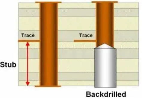
A typical PTH consists of three parts: a drilled hole through the PCB substrate, a copper plating layer covering the hole wall, and pads on the top and bottom surfaces of the PCB. In multi-layer PCBs, a PTH may only need to connect a few specific layers (e.g., layers 2 and 5 in an 8-layer PCB), leaving the unused portions of the hole wall—known as stubs—extending beyond the target layers.
1.2 Parasitic Effects of Unused PTH Stubs in High-Speed Systems
At low signal frequencies (below 1 Gbps), the parasitic capacitance and inductance of PTH stubs are negligible and do not affect signal quality. However, when signal rates exceed 10 Gbps, the wavelength of the signal becomes comparable to the length of the stub, and the stub behaves like an open-circuited transmission line, leading to three critical signal integrity issues:
- Signal Reflection: The impedance discontinuity at the junction of the stub and the main signal path causes part of the signal to be reflected back to the source, resulting in signal waveform distortion and reduced signal-to-noise ratio (SNR).
- Insertion Loss: The stub acts as a resonant cavity at specific frequencies, absorbing signal energy and increasing attenuation, which shortens the effective transmission distance of high-speed signals.
- Crosstalk Enhancement: Unused stubs increase the coupling area between adjacent PTHs, intensifying electromagnetic interference (EMI) between high-speed signal paths and further degrading signal quality.
The severity of these effects is directly proportional to the length of the stub. For example, a 500μm long stub can cause a 20% increase in signal reflection and a 15% increase in insertion loss at 25 Gbps, which is sufficient to cause communication errors in high-speed serial links such as PCIe 4.0 and 100G Ethernet. Back drilling solves these problems by removing the unused stub sections, eliminating impedance discontinuities and restoring the integrity of the high-speed signal path.
2. Core Principles and Implementation Process of Back Drilling Technology
Back drilling is a precision mechanical drilling process that targets and removes unused PTH stubs after the completion of PCB plating and lamination. Its core principle is to align the drill bit with the center of the PTH and control the drilling depth with high precision, ensuring that only the stub portion is removed without damaging the target conductive layers or the PCB substrate.
2.1 Key Principles of Back Drilling
The implementation of back drilling relies on two core technical principles:
- Precision Depth Control: The drill bit must stop precisely at the boundary between the unused stub and the target conductive layer. This requires the drilling machine to have a depth control accuracy of ±25μm or higher, which is far stricter than standard PCB drilling (±100μm).
- Coaxial Alignment: The back drill bit must be perfectly coaxial with the original PTH. Any offset (concentricity deviation) between the drill bit and the PTH will cause partial removal of the target conductive layer or incomplete removal of the stub, both of which will compromise signal integrity. IPC-6012 specifies that the maximum allowable concentricity deviation for back drilling is ±50μm for Class 3 high-reliability PCBs.
Unlike standard PCB drilling, which aims to create through-holes, back drilling is a blind drilling process that only penetrates part of the PCB thickness. The depth of the back drill hole is determined by the formula:  Where:
Where:- Dbd = Back drilling depth
- Tpcb = Total thickness of the PCB
- Dt1= Distance from the bottom surface of the PCB to the lower target layer
- Dt2= Safety margin (typically 50–100μm) to prevent damage to the target layer
2.2 Step-by-Step Implementation Process of Back Drilling
Back drilling is integrated into the PCB manufacturing process after the completion of PTH plating and before solder mask application. The detailed implementation steps are as follows:
- Pre-Drilling and Plating: First, the standard PTH drilling and copper plating process is completed. The hole wall is plated with copper to form a conductive layer, and the pads on the top and bottom surfaces are formed by etching. At this stage, the PTH is a full-through hole with unused stubs extending beyond the target layers.
- Target Layer Position Calibration: Use a high-precision optical positioning system to scan the PCB and determine the exact position of the target conductive layers connected by the PTH. This step is critical for multi-layer PCBs, as layer-to-layer registration errors can lead to inaccurate back drilling depth.
- Back Drill Bit Selection: Choose a drill bit with a diameter 10–20% larger than the diameter of the original PTH. A slightly larger drill bit ensures that the entire stub is removed, including the copper plating on the hole wall. For example, a 0.5mm diameter PTH requires a 0.55–0.6mm diameter back drill bit.
- Precision Depth Drilling: Mount the PCB on a CNC back drilling machine, align the drill bit with the center of the PTH, and set the drilling depth according to the calculated value. The drilling machine uses a servo motor to control the feed rate of the drill bit (typically 0.1–0.5 mm/s) to ensure depth accuracy. During drilling, compressed air is used to remove drilling debris and cool the drill bit, preventing substrate damage from heat.
- Stub Removal Inspection: After drilling, inspect the back-drilled holes using an automated optical inspection (AOI) system or a digital microscope. Check two key indicators: whether the stub has been completely removed, and whether the target conductive layer has been damaged. For high-reliability applications, cross-sectional analysis may be performed to verify the quality of the back-drilled hole.
- Deburring and Cleaning: Remove any residual copper debris or burrs from the back-drilled holes using a chemical etching or mechanical polishing process. Clean the PCB with deionized water to remove drilling residues, ensuring that no contaminants remain in the holes.
- Solder Mask Application: Apply solder mask to the PCB surface, covering the pads and the back-drilled holes to prevent oxidation and short circuits.
2.3 Classification of Back Drilling Technology
Based on the drilling direction and the number of stubs removed, back drilling is divided into two main types:
- Single-Side Back Drilling: Drilling from one side of the PCB to remove a single unused stub. This is the most common type, suitable for PTHs that only need to connect layers close to one side of the PCB (e.g., layers 3–6 in a 10-layer PCB, with the stub extending to the bottom surface).
- Double-Side Back Drilling: Drilling from both the top and bottom sides of the PCB to remove two unused stubs. This is used for PTHs that connect intermediate layers (e.g., layers 4–7 in a 12-layer PCB), with stubs extending to both the top and bottom surfaces. Double-side back drilling requires higher alignment accuracy to ensure that the two drill holes do not intersect and damage the target layers.
3. Key Technical Parameters and Quality Control Standards for Back Drilling
The quality of back drilling directly determines its effectiveness in improving signal integrity. To ensure consistent and reliable performance, several key technical parameters must be strictly controlled during the manufacturing process, in accordance with international industry standards.
3.1 Critical Technical Parameters
- Depth Accuracy: The most important parameter for back drilling, defined as the difference between the actual drilling depth and the target depth. For high-speed PCBs, the depth accuracy must be controlled within ±25μm. Excessive depth will damage the target conductive layer, while insufficient depth will leave residual stub segments, both of which will compromise signal quality.
- Concentricity Deviation: The offset between the center of the back drill hole and the center of the original PTH. As specified in IPC-6012, the maximum allowable concentricity deviation is ±50μm for Class 3 PCBs and ±75μm for Class 2 PCBs. A large deviation will cause uneven removal of the stub and may damage the pad.
- Drill Bit Diameter Tolerance: The diameter of the back drill bit must be 10–20% larger than the original PTH diameter, with a tolerance of ±0.02mm. A bit that is too small cannot completely remove the stub, while a bit that is too large will damage the surrounding copper traces and pads.
- Surface Roughness of Back-Drilled Holes: The surface roughness (Ra) of the hole wall after back drilling must be ≤1.6μm. A rough surface will increase signal loss and may cause solder mask adhesion problems.
- Residual Stub Length: The maximum allowable length of residual stubs after back drilling is ≤50μm for signals above 25 Gbps. Residual stubs longer than this will still introduce significant parasitic effects.
3.2 Quality Control Standards and Inspection Methods
The quality of back-drilled PCBs is governed by two core standards: IPC-6012 (Qualification and Performance Specification for Rigid Printed Boards) and IPC-A-600 (Acceptability of Printed Boards). The main inspection methods include:
- Automated Optical Inspection (AOI): Uses high-resolution cameras to scan the back-drilled holes, detecting residual stubs, concentricity deviations, and pad damage. AOI can inspect 100% of the back-drilled holes in high-volume production, with a detection accuracy of 99% or higher.
- Cross-Sectional Analysis: For prototype PCBs or high-reliability applications, cut the PCB perpendicular to the back-drilled hole and polish the cross-section. Use a metallographic microscope to measure the depth of the back drill hole, the length of residual stubs, and the integrity of the target conductive layer. This is the most accurate inspection method but is destructive and time-consuming.
- Electrical Testing: Measure the impedance and insertion loss of the back-drilled PTH using a network analyzer. Compare the test results with the simulation data to verify whether the back drilling has effectively eliminated parasitic effects. For 25 Gbps signals, the insertion loss should be reduced by at least 10% after back drilling.
4. Application Scenarios of Back Drilling Technology
Back drilling is not a universal technology for all PCBs; it is specifically designed for high-speed, high-frequency electronic systems where signal integrity is a critical requirement. Below are the key application scenarios where back drilling is indispensable.
4.1 Data Center and Telecommunication Equipment
Data centers and telecommunication networks are the largest application areas for back drilling technology, as they rely on high-speed serial links to transmit massive amounts of data. Specific applications include:
- 100G/400G Ethernet Switches: The backplanes of these switches use PTHs to connect line cards and control cards, with signal rates of 25 Gbps per lane. Back drilling removes stubs to ensure that the signal reflection coefficient is less than -20 dB, meeting the requirements of the IEEE 802.3bj standard.
- 5G Base Stations: 5G active antenna units (AAUs) and baseband units (BBUs) operate at frequencies of 3.5 GHz to 28 GHz. Back drilling reduces the parasitic capacitance of PTHs, improving the isolation between RF signals and reducing EMI.
- Storage Area Networks (SANs): Devices such as Fibre Channel switches use 16 Gbps and 32 Gbps serial links, where back drilling is required to maintain signal integrity over long transmission distances.
In these applications, back drilling is often combined with other high-speed PCB design techniques, such as impedance-controlled traces and differential pairs, to achieve optimal signal performance.
4.2 Aerospace and Defense Electronics
Aerospace and defense systems have strict requirements for reliability and signal integrity, especially in harsh environments with high vibration and temperature fluctuations. Back drilling is widely used in:
- Avionics Systems: Flight control computers, radar systems, and satellite communication equipment use high-speed PCBs with PTHs connecting multiple layers. Back drilling eliminates stub-induced signal distortion, ensuring the accuracy of flight data transmission and radar signal processing.
- Military Communication Devices: Tactical radios and secure communication systems operate at high frequencies, where EMI is a major concern. Back drilling reduces the coupling between PTHs, improving the anti-interference ability of the system.
For aerospace applications, back-drilled PCBs must meet IPC-6012 Class 3 standards, with 100% cross-sectional inspection to ensure zero defects.
4.3 High-Performance Computing (HPC)
High-performance computing systems, such as supercomputers and AI training servers, require massive parallel data transmission between processors and memory modules. Back drilling plays a key role in:
- CPU/Memory Interconnects: The PCBs connecting CPUs and DDR5 memory modules use PTHs to transmit high-speed signals at 3200 Mbps or higher. Back drilling removes stubs to reduce signal reflection and improve the stability of memory access.
- GPU Accelerator Cards: Modern GPUs use PCIe 5.0 interfaces with a signal rate of 32 Gbps per lane. Back drilling is required for the PTHs on the accelerator card to meet the strict impedance requirements of PCIe 5.0.
In HPC systems, back drilling is often used in conjunction with buried vias and blind vias to minimize the number of through-holes and further improve signal integrity.
4.4 Medical Electronics
High-end medical devices require precise signal processing and data transmission, making back drilling an essential technology in:
- Magnetic Resonance Imaging (MRI) Machines: The RF coils of MRI machines use PCBs with PTHs to transmit high-frequency signals. Back drilling reduces parasitic inductance, improving the signal-to-noise ratio of the MRI images.
- Ultrasound Equipment: The transducer arrays of ultrasound machines use multi-layer PCBs, where back drilling eliminates stub-induced signal distortion, ensuring the accuracy of ultrasonic wave emission and reception.
Medical devices using back-drilled PCBs must comply with ISO 13485 standards, with strict traceability of the manufacturing process.
5. Advantages, Limitations, and Future Trends of Back Drilling Technology
While back drilling is highly effective for improving high-speed signal integrity, it also has inherent advantages and limitations that must be considered in PCB design. Additionally, as electronic systems continue to evolve, back drilling technology is undergoing continuous innovation.
5.1 Key Advantages of Back Drilling
- Improved Signal Integrity: The most significant advantage of back drilling is the elimination of stub-induced parasitic effects, reducing signal reflection, insertion loss, and crosstalk. For 25 Gbps signals, back drilling can improve the signal-to-noise ratio by 15–20 dB.
- Cost-Effective Solution: Compared to alternative technologies such as buried vias and blind vias, back drilling is a lower-cost option, as it uses standard PCB manufacturing equipment with minimal modifications. This makes it suitable for high-volume production.
- Compatibility with Standard Processes: Back drilling can be integrated into the standard PCB manufacturing process without requiring special materials or equipment. This allows PCB manufacturers to easily adopt the technology without significant capital investment.
5.2 Limitations of Back Drilling
- Depth Control Challenges: Achieving ±25μm depth accuracy requires high-precision CNC drilling machines, which are expensive and may not be available to all PCB manufacturers.
- Risk of Target Layer Damage: Even a small depth error can damage the target conductive layer, leading to open circuits and PCB failure. This requires strict quality control during the drilling process.
- Limited Applicability to Thin PCBs: For PCBs with a total thickness of less than 0.8mm, the stub length is too short to justify back drilling, as the parasitic effects are negligible.
- Increased Manufacturing Time: Back drilling adds an additional step to the PCB manufacturing process, increasing production time by 10–15%. This may affect delivery schedules for high-volume orders.
5.3 Future Development Trends
As signal rates continue to increase (towards 100 Gbps and beyond), back drilling technology is evolving in three key directions:
- Laser Back Drilling: Replacing mechanical drill bits with laser beams for more precise depth control and smaller concentricity deviation. Laser back drilling can achieve a depth accuracy of ±10μm and is suitable for microvias with diameters less than 0.2mm.
- Automated In-Line Back Drilling: Integrating back drilling machines into the PCB production line, enabling real-time depth adjustment and quality inspection. This reduces production time and improves process consistency.
- Combination with 3D Printing: Using 3D printing technology to fabricate PCBs with pre-defined via structures, eliminating the need for post-processing back drilling. This is still in the experimental stage but has the potential to revolutionize high-speed PCB manufacturing.
6. Conclusion
Back drilling technology has become an indispensable part of high-speed PCB design, addressing the critical signal integrity challenges posed by unused PTH stubs in modern electronic systems. By precisely removing these stubs, back drilling eliminates impedance discontinuities, reduces signal reflection and attenuation, and improves the overall performance and reliability of high-speed communication devices. Its implementation relies on strict control of depth accuracy, concentricity deviation, and other key parameters, in accordance with IPC industry standards.
While back drilling has limitations in terms of manufacturing complexity and cost, its advantages in improving signal integrity far outweigh these drawbacks for high-speed applications such as data centers, 5G base stations, and aerospace electronics. As signal rates continue to rise, the development of laser back drilling and automated in-line processes will further enhance the precision and efficiency of this technology, enabling it to meet the ever-growing demands of next-generation electronic systems.