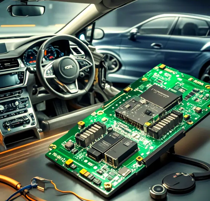
Automotive electronIC PCBs are the "nerve centers" of modern vehicles, controlling critical systems such as powertrains, advanced driver-assistance systems (ADAS), and braking. Among these PCBs, safety-critical components—including microcontrollers (MCUs) (e.g., automotive-grade MCU series like NXP S32K) and sensors (e.g., radar, LiDAR, and pressure sensors)—are responsible for processing safety-related data and executing life-saving commands. Their reliability directly impacts vehicle safety, as defined by standards such as ISO 26262 (functional safety for road vehicles). In contrast, high-noise components—such as motor drivers (e.g., MOSFET/IGBT-based motor controllers), DC-DC converters, and ignition modules—generate intense electromagnetic inteRFerence (EMI) and voltage/current transients. These interferences manifest in two primary forms:
- Electromagnetic radiation: High-frequency switching (100kHz–100MHz) in motor drivers emits radiated EMI, which can disrupt sensor signal acquisition (e.g., causing radar sensor false triggers).
- Conducted noise: Voltage spikes (up to 100V) from motor load changes propagate through power/ground traces, leading to MCU power supply instability (e.g., resetting the MCU during critical braking operations).
The distance between safety-critical and high-noise components is a key design parameter for mitigating these risks. A poorly defined distance can increase EMI coupling by 20–40%, raising the likelihood of safety-related failures (e.g., ADAS misinterpreting obstacles). Thus, establishing science-based distance guidelines is essential for complying with ISO 26262 and ensuring vehicle safety.
Before defining specific distances, it is critical to understand the two primary EMI coupling mechanisms that distance mitigates, as well as the safety requirements that govern design:
- Far-field radiation coupling: Follows the inverse-square law—radiated EMI intensity decreases with the square of the distance from the noise source. For example, a motor driver emitting 100μV/m of EMI at 10cm will only emit 25μV/m at 20cm.
- Near-field capacitive/inductive coupling: Dominates at short distances (<λ/2π, where λ is the wavelength of the noise frequency). Capacitive coupling (between traces) and inductive coupling (between current loops) decrease exponentially with distance, making small distance increases (e.g., 5mm to 10mm) highly effective at reducing coupling.
ISO 26262 classifies automotive components into ASIL (Automotive Safety Integrity Level) grades (A–D), with ASIL D representing the highest safety criticality (e.g., autonomous braking MCUs). Higher ASIL grades demand stricter EMI mitigation, including larger distances between safety and noise components:
- ASIL A/B (e.g., climate control sensors): Acceptable EMI coupling margin of 10–15dB.
- ASIL C/D (e.g., ADAS radar MCUs): Required EMI coupling margin of ≥20dB.
These margins directly translate to distance requirements—higher margins need larger distances to suppress EMI to safe levels.
The required distance depends on three factors: the type of high-noise component, the ASIL grade of the safety component, and the PCB layer stackup (e.g., presence of ground planes). Below are industry-validated distance guidelines for common component pairings:
MCUs process digital/analog safety data and are highly sensitive to power supply noise and radiated EMI. Motor drivers (e.g., for electric power steering or window motors) are the most potent noise sources in automotive PCBs, with switching frequencies of 50kHz–2MHz and current transients of 10–50A.
Example: An ASIL D MCU (e.g., for autonomous driving) paired with a 50A motor driver must be at least 25mm apart on the same layer. If separated by a solid ground plane (0.3mm thick), the distance can be reduced to 18mm—still ensuring EMI levels stay below the MCU’s noise immunity threshold (typically ±50mV for power supplies).
Sensors (e.g., radar, LiDAR, and wheel-speed sensors) output low-amplitude analog signals (mV level), making them even more sensitive to EMI than MCUs. For example, a wheel-speed sensor signal (10–100mV) can be completely masked by motor driver noise if distances are insufficient.
- High-power motor drivers (>50A): Increase distances by 20–30%. For example, a 100A motor driver (e.g., for EV traction control) paired with an ASIL D MCU requires a minimum distance of 30–39mm (up from 25–30mm for 50A drivers).
- PCB with no ground plane (rare in automotive): Double the distance. Without a ground plane to shield EMI, an ASIL C MCU and motor driver need 50–60mm of separation (up from 25–30mm with a ground plane).
- Flexible PCBs (FPCs) for in-cabin sensors: Increase distances by 15–20%. FPCs have thinner substrates and weaker EMI shielding, so an ASIL B sensor needs 23–30mm of distance from a motor driver (up from 20–25mm on rigid PCBs).
While distance is critical, it must be paired with other EMI mitigation strategies to meet ISO 26262 requirements. These measures reduce reliance on extreme distances (which may be impractical in space-constrained automotive PCBs):
- Use a solid ground plane between safety and noise components (if on different layers). This creates an EMI "barrier" that reduces coupling by 15–25dB, allowing distance reductions of 30–40%.
- For multi-layer PCBs, route safety component grounds to a dedicated ground plane, and noise component grounds to a separate power ground plane—avoiding ground loop-induced noise.
- Add metal shields (e.g., copper cans) around high-noise motor drivers. Shields can reduce radiated EMI by 30–40dB, allowing distance reductions of 50% (e.g., from 25mm to 12.5mm for an ASIL D MCU).
- Install EMI filters (e.g., ferrite beads, ceramic capacitors) on motor driver power inputs and sensor signal lines. A 100nF X7R capacitor (for power filtering) and a 100Ω ferrite bead (for signal filtering) can reduce conducted noise by 20–30dB.
- Route safety component traces (e.g., sensor signals) perpendicularly to high-noise traces (e.g., motor driver power lines). Perpendicular routing reduces capacitive coupling by 50–70% compared to parallel routing.
- Keep high-noise traces (e.g., motor driver current paths) as short as possible (<20mm) to minimize EMI radiation loops. Shorter loops reduce the area of the "antenna" emitting EMI.
To confirm that distance and mitigation measures are effective, automotive PCB designers must conduct two key validation steps:
- Use electromagnetic simulation tools (e.g., ANSYS HFSS, CST Studio Suite) to model EMI coupling between safety and noise components. Simulations should verify that:
- Radiated EMI at the safety component location is below the CISPR 25 Class 5 limit (≤30dBμV/m at 10m for 30–1000MHz).
- Conducted noise on safety component power traces is below ±50mV (for ASIL C/D) or ±100mV (for ASIL A/B).
- Perform EMI immunity testing per ISO 11452 (automotive EMI testing). For example, inject radiated EMI (up to 200V/m) near high-noise components and verify that safety components (e.g., MCU, sensors) continue to operate correctly.
- Measure signal integrity of sensor outputs using an oscilloscope. For a wheel-speed sensor, the signal-to-noise ratio (SNR) should be ≥20dB—confirming that distance and filtering have suppressed noise effectively.
 PCB
PCB FPC
FPC Rigid-Flex
 FR-4
FR-4 HDI PCB
 Rogers High-Frequency Board
 PTFE Teflon High-Frequency Board
 Aluminum
 Copper Core
 PCB Assembly
 LED light PCBA
 Memory PCBA
 Power Supply PCBA
 New Energey PCBA
 Communication PCBA
 Industrial Control PCBA
 Medical Equipment PCBA
 Testing Service
 PCBA Testing Service
 Certification Application
 RoHS Certification Application
 REACH Certification Application
 CE Certification Application
 FCC Certification Application
 CQC Certification Application
 UL Certification Application
 Transformers, Inductors
 High Frequency Transformers
 Low Frequency Transformers
 High Power Transformers
 Conversion Transformers
 Sealed Transformers
 Ring Transformers
 Inductors
 Wires,Cables Customized
 Network Cables
 Power Cords
 Antenna Cables
 Coaxial Cables
 Net Position Indicator
 Solar AIS net position indicator
 Capacitors
 Connectors
 Diodes
 Embedded Processors & Controllers
 Digital Signal Processors (DSP/DSC)
 Microcontrollers (MCU/MPU/SOC)
 Programmable Logic Device(CPLD/FPGA)
 Communication Modules/IoT
 Resistors
 Through Hole Resistors
 Resistor Networks, Arrays
 Potentiometers,Variable Resistors
 Aluminum Case,Porcelain Tube Resistance
 Current Sense Resistors,Shunt Resistors
 Switches
 Transistors
 Power Modules
 Isolated Power Modules
 AC-DC Power Modules
 DC-AC Module(Inverter)
 RF and Wireless