 PCB
PCB FPC
FPC Rigid-Flex
 FR-4
FR-4 HDI PCB
 Rogers High-Frequency Board
 PTFE Teflon High-Frequency Board
 Aluminum
 Copper Core
 PCB Assembly
 LED light PCBA
 Memory PCBA
 Power Supply PCBA
 New Energey PCBA
 Communication PCBA
 Industrial Control PCBA
 Medical Equipment PCBA
 Testing Service
 PCBA Testing Service
 Certification Application
 RoHS Certification Application
 REACH Certification Application
 CE Certification Application
 FCC Certification Application
 CQC Certification Application
 UL Certification Application
 Transformers, Inductors
 High Frequency Transformers
 Low Frequency Transformers
 High Power Transformers
 Conversion Transformers
 Sealed Transformers
 Ring Transformers
 Inductors
 Wires,Cables Customized
 Network Cables
 Power Cords
 Antenna Cables
 Coaxial Cables
 Net Position Indicator
 Solar AIS net position indicator
 Capacitors
 Connectors
 Diodes
 Embedded Processors & Controllers
 Digital Signal Processors (DSP/DSC)
 Microcontrollers (MCU/MPU/SOC)
 Programmable Logic Device(CPLD/FPGA)
 Communication Modules/IoT
 Resistors
 Through Hole Resistors
 Resistor Networks, Arrays
 Potentiometers,Variable Resistors
 Aluminum Case,Porcelain Tube Resistance
 Current Sense Resistors,Shunt Resistors
 Switches
 Transistors
 Power Modules
 Isolated Power Modules
 AC-DC Power Modules
 DC-AC Module(Inverter)
 RF and Wireless
Improving Copper Plating Uniformity in High-Aspect-Ratio Vias via Atomic Layer Deposition (ALD)
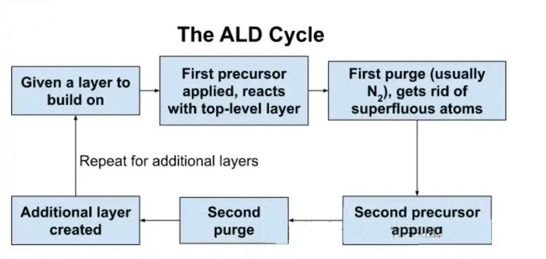
1. Principles and Advantages of ALD
Atomic Layer Deposition (ALD) employs self-limiting suRFace reactions to deposit conformal thin films (conformality >95%) through alternating precursor pulses (e.g., Cu(hfac)₂, H₂O). For high-aspect-ratio (AR>10:1) vias, ALD offers:
-
3D uniformity: Eliminates shadow effects via layer-by-layer growth, ensuring coverage at via bottoms, sidewalls, and tops;
-
Ultrathin seed layers: 2–5 nm continuous copper layers reduce activation overpotential for subsequent electroplating;
-
Interface engineering: Nanoscale barrier/seed stacks (e.g., TaN/Cu) suppress copper diffusion.
2. Key Technical Approaches
(1) Precursor and Reaction Optimization
-
Precursor selection:
-
Copper precursors: β-diketonates (e.g., Cu(acac)₂) or cyclopentadienyl compounds (e.g., CpCuPEt₃) enable efficient reactions at 150–300°C;
-
Reductants: H₂ or plasma-assisted H₂ (PE-ALD) enhance reduction efficiency, minimizing carbon residues (<5 at.%).
-
-
Pulse design:
-
Extended precursor pulse (1–5 s) and purge times (5–10 s) ensure deep via penetration;
-
Pressure gradient (0.1–1 Torr) improves precursor transport.
-
(2) Seed Layer Morphology and Electrical Tuning
-
Nano-grain control:
-
Low-temperature ALD (<200°C) produces nanocrystalline Cu (5–10 nm grains), lowering electroplating nucleation barriers;
-
Organic additives (e.g., SPS, PEG) modify surface energy for uniform plating.
-
-
Resistivity reduction:
-
In-situ plasma annealing (300°C, N₂/H₂) lowers resistivity to 2–3 μΩ·cm (near bulk Cu’s 1.7 μΩ·cm).
-
(3) Synergistic Electroplating Design
-
Pulse-reverse electroplating (PRC):
-
Optimize forward current density (1–5 mA/cm²) and pulse ratios (Ton/Toff=10:1) to suppress "dog-boning";
-
Balance deposition rates with accelerators (SPS) and inhibitors (PEG).
-
(4) Transport Dynamics Modeling
-
CFD SIMulations:
-
Model precursor diffusion/adsorption in vias to optimize pulse parameters;
-
-
Monte Carlo surface reaction models:
-
Predict ALD coverage and define critical AR limits (AR_max≈50:1).
-
3. Validation and Performance Metrics
-
Conformality tests:
-
TEM cross-sections show <±5% thickness variation in AR=20:1 vias (vs. >±30% for PVD);
-
-
Plating results:
-
ALD seeds achieve >95% bottom-up filling in AR=15:1 vias (vs. 70% for PVD);
-
-
Reliability:
-
Post-thermal cycling (-55–125°C, 1000×), resistance drift <2% with no voids/cracks.
-
4. Challenges and Solutions
-
Challenge 1: Precursor thermal instability:
-
Solution: Develop thermally stable precursors (e.g., Cu(I) amides) for >300°C processes;
-
-
Challenge 2: Precursor depletion in deep vias:
-
Solution: Synchronized pumping to maintain concentration gradients;
-
-
Challenge 3: Low ALD growth rate (<0.1 nm/cycle):
-
Solution: Spatial ALD boosts rates to >1 nm/s for high-throughput production.
-
5. Applications and Economics
-
3D TSV packaging: ALD enables void-free filling in AR=30:1 vias, increasing interconnect density 5×;
-
Advanced nodes (<5 nm): Reduces RC delay by 20% in dual damascene interconnects;
-
Cost analysis: Higher ALD tool cost (+30%) offset by yield gains (>95% vs. 80%) and material savings (-15% Cu usage).