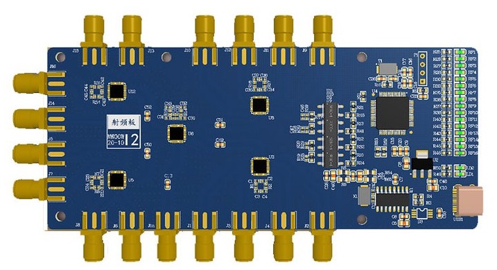
Radio Frequency (RF) PCBs are the backbone of wireless communication devices—including smartphones, Wi-Fi routers, Bluetooth modules, and 5G transceivers—where signal integrity directly dictates communication range, data rate, and power efficiency. The signal path between the RF chip (e.g., transceivers, power amplifiers) and the Antenna is the most critical section of the RF PCB, as any inefficiency here translates directly to signal loss (attenuation). RF signals propagate from the chip to the antenna via transmission lines (e.g., microstrip, coplanar waveguide), and the layout distance between the two components influences two key sources of attenuation:
- Transmission line loss: Signal energy dissipates as it travels along the line, increasing with length due to conductor resistance, dielectric loss, and radiation leakage.
- Impedance mismatch: Longer distances raise the risk of trace discontinuities (e.g., bends, vias) that disrupt the 50Ω characteristic impedance, causing reflections and additional attenuation.
A 3dB attenuation increase is a critical threshold—it halves the signal power, reducing communication range by ~30% (for free-space propagation) or doubling the required transmit power (shortening battery life in portable devices). Thus, defining the distance threshold that triggers this 3dB loss is essential for optimizing RF PCB performance.
Before establishing distance thresholds, it is critical to understand the variables that modify how distance impacts attenuation. These factors must be considered alongside raw distance to avoid oversimplification:
Higher frequencies experience greater attenuation due to increased skin effect (conductor loss) and dielectric loss. For example:
- Low RF (300MHz–1GHz, e.g., FM radio, Bluetooth Classic): Low transmission line loss (~0.2–0.5dB/cm).
- Mid RF (1–6GHz, e.g., Wi-Fi 6, 4G LTE): Moderate loss (~0.5–1.0dB/cm).
- High RF (6–30GHz, e.g., 5G mmWave, satellite communication): High loss (~1.0–3.0dB/cm).
The choice of transmission line affects loss per unit length:
- Microstrip: The most common RF line, with loss increasing with narrower width (to maintain 50Ω impedance). A 0.2mm-wide microstrip on 0.8mm FR-4 has ~0.8dB/cm loss at 5GHz.
- Coplanar Waveguide (CPW): Lower radiation loss than microstrip but higher conductor loss (~1.0dB/cm at 5GHz for similar dimensions).
- Stripline: Embedded in the PCB, with lower radiation loss but higher dielectric loss (~0.7dB/cm at 5GHz on FR-4).
RF-optimized materials reduce loss compared to standard FR-4:
- Standard FR-4: εᵣ=3.8–4.5, tanδ=0.015–0.02 (high loss, ~0.8dB/cm at 5GHz).
- PTFE (Teflon): εᵣ=2.1–2.3, tanδ=0.001–0.002 (low loss, ~0.3dB/cm at 5GHz).
- Ceramic-filled laminates (e.g., Rogers RO4350): εᵣ=3.48, tanδ=0.0037 (balanced loss, ~0.4dB/cm at 5GHz).
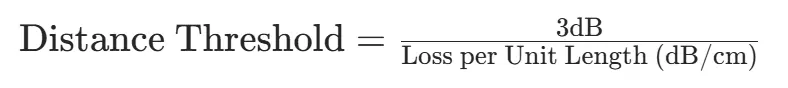
The distance at which attenuation exceeds 3dB is calculated as:
Below are industry-validated distance thresholds for common RF bands and PCB materials, assuming 50Ω transmission lines with minimal discontinuities (no sharp bends, ≤1 via):
Low frequencies are least sensitive to distance, with thresholds exceeding 10cm for most materials:
Example: A Bluetooth Classic (2.4GHz is mid-RF, but 900MHz is low-RF) module on FR-4 can have a 12cm chip-antenna distance before attenuation hits 3dB.
This is the most common range for consumer electronics, with thresholds typically between 3–10cm:
Critical Observation: For Wi-Fi 6 (5GHz) on standard FR-4—a common smartphone/ router scenario—the 3dB threshold is just 3–3.75cm. Exceeding this (e.g., a 5cm distance) increases attenuation to 4–5dB, halving signal power.
High frequencies are extremely sensitive to distance, with thresholds often <5cm even for low-loss materials:
Example: A 5G mmWave (28GHz) module on Rogers RO4350 cannot have a chip-antenna distance exceeding 3cm without losing >3dB of signal power.
Certain design choices or environmental factors can lower the 3dB distance threshold by increasing loss per unit length. These scenarios require shorter chip-antenna distances:
- Sharp bends (>90°): Each sharp bend adds 0.2–0.5dB loss. A 5GHz FR-4 path with two 90° bends has loss ~1.2–1.5dB/cm, reducing the 3dB threshold to 2–2.5cm.
- Vias: A single via (through-hole) adds 0.3–0.8dB loss at 5GHz. A path with one via has loss ~1.1–1.8dB/cm, lowering the threshold to 1.7–2.7cm.
Crowded RF PCBs increase crosstalk (signal leakage between adjacent traces) and radiation loss. For example, a 5GHz FR-4 path surrounded by digital components has ~1.2dB/cm loss, reducing the 3dB threshold to 2.5cm.
Flexible substrates (e.g., PI with εᵣ=3.2, tanδ=0.008) have higher loss than rigid RF materials. A 5GHz PI path has ~0.9–1.1dB/cm loss, reducing the 3dB threshold to 2.7–3.3cm (vs. 3–3.75cm for FR-4).
When space constraints force longer chip-antenna distances, these techniques reduce loss and avoid the 3dB threshold:
Upgrading from FR-4 to Rogers RO4350 or PTFE can double the distance threshold. For 5GHz, this extends the threshold from 3–3.75cm (FR-4) to 6–10cm (PTFE).
- Widen microstrips: For 50Ω impedance on 0.8mm FR-4, a 0.4mm-wide microstrip has ~0.6dB/cm loss (vs. 0.8dB/cm for 0.2mm), extending the 3dB threshold to 5cm.
- Add ground planes: A double-sided ground plane (top and bottom of the transmission line) reduces radiation loss by 30–40%, lowering loss to ~0.5–0.7dB/cm at 5GHz (threshold: 4.3–6cm).
A compact RF power amplifier (e.g., 2dB gain) in the chip-antenna path compensates for transmission line loss. For a 5cm FR-4 path (loss ~4dB at 5GHz), a 2dB amplifier reduces net attenuation to 2dB, staying below the 3dB threshold.
- Use 45° bends instead of 90° bends (adds <0.1dB loss per bend).
- Use vias instead of through-holes (reduce via loss by 50%).
To confirm that chip-antenna distance does not exceed the 3dB threshold, perform these tests:
- Connect a VNA to the RF chip’s output and the antenna port. Sweep the frequency range and measure insertion loss (IL) along the transmission line.
- Ensure IL ≤3dB at the target frequency (e.g., 5GHz for Wi-Fi).
- Measure the antenna’s effective isotropic radiated power (EIRP) at different chip-antenna distances. A 3dB drop in EIRP indicates the distance threshold has been exceeded.
- For end devices (e.g., smartphones), measure maximum communication range at varying distances. A 30% range reduction correlates to a 3dB attenuation increase.
The distance threshold between an RF chip and antenna that causes >3dB signal attenuation depends heavily on frequency and PCB material:
- Low RF (300MHz–1GHz): 10–37.5cm (FR-4 to PTFE).
- Mid RF (1–6GHz): 3–10cm (FR-4 to PTFE)—critical for consumer electronics like Wi-Fi 6 devices.
- High RF (6–30GHz): 1–3.75cm (FR-4 to PTFE)—stringent for 5G mmWave.
Discontinuities (bends, vias) and high-density layouts reduce these thresholds, while low-loss materials, optimized transmission lines, and RF amplifiers extend them. For RF PCB designers, balancing distance with these mitigation strategies is essential to avoid the 3dB attenuation cliff—ensuring devices deliver reliable wireless performance without sacrificing power efficiency or range.
As RF frequencies continue to rise (e.g., 6G’s 100GHz bands), future designs will rely on integrated antenna-chip modules (reducing distance to <1cm) and advanced materials (e.g., graphene-based transmission lines) to manage attenuation, pushing the boundaries of what is possible in compact RF systems.
 PCB
PCB FPC
FPC Rigid-Flex
 FR-4
FR-4 HDI PCB
 Rogers High-Frequency Board
 PTFE Teflon High-Frequency Board
 Aluminum
 Copper Core
 PCB Assembly
 LED light PCBA
 Memory PCBA
 Power Supply PCBA
 New Energey PCBA
 Communication PCBA
 Industrial Control PCBA
 Medical Equipment PCBA
 Testing Service
 PCBA Testing Service
 Certification Application
 RoHS Certification Application
 REACH Certification Application
 CE Certification Application
 FCC Certification Application
 CQC Certification Application
 UL Certification Application
 Transformers, Inductors
 High Frequency Transformers
 Low Frequency Transformers
 High Power Transformers
 Conversion Transformers
 Sealed Transformers
 Ring Transformers
 Inductors
 Wires,Cables Customized
 Network Cables
 Power Cords
 Antenna Cables
 Coaxial Cables
 Net Position Indicator
 Solar AIS net position indicator
 Digital Signal Processors (DSP/DSC)
 Microcontrollers (MCU/MPU/SOC)
 Programmable Logic Device(CPLD/FPGA)
 Through Hole Resistors
 Resistor Networks, Arrays
 Potentiometers,Variable Resistors
 Aluminum Case,Porcelain Tube Resistance
 Current Sense Resistors,Shunt Resistors
 Isolated Power Modules
 AC-DC Power Modules
 DC-AC Module(Inverter)
 Capacitors
  Connectors
  Diodes
 Embedded Processors & Controllers
 Communication Modules/IoT
 Resistors
 Switches
 Transistors
 Power Modules
 RF and Wireless