 PCB
PCB FPC
FPC Rigid-Flex
 FR-4
FR-4 HDI PCB
 Rogers High-Frequency Board
 PTFE Teflon High-Frequency Board
 Aluminum
 Copper Core
 PCB Assembly
 LED light PCBA
 Memory PCBA
 Power Supply PCBA
 New Energey PCBA
 Communication PCBA
 Industrial Control PCBA
 Medical Equipment PCBA
 Testing Service
 PCBA Testing Service
 Certification Application
 RoHS Certification Application
 REACH Certification Application
 CE Certification Application
 FCC Certification Application
 CQC Certification Application
 UL Certification Application
 Transformers, Inductors
 High Frequency Transformers
 Low Frequency Transformers
 High Power Transformers
 Conversion Transformers
 Sealed Transformers
 Ring Transformers
 Inductors
 Wires,Cables Customized
 Network Cables
 Power Cords
 Antenna Cables
 Coaxial Cables
 Net Position Indicator
 Solar AIS net position indicator
 Capacitors
 Connectors
 Diodes
 Embedded Processors & Controllers
 Digital Signal Processors (DSP/DSC)
 Microcontrollers (MCU/MPU/SOC)
 Programmable Logic Device(CPLD/FPGA)
 Communication Modules/IoT
 Resistors
 Through Hole Resistors
 Resistor Networks, Arrays
 Potentiometers,Variable Resistors
 Aluminum Case,Porcelain Tube Resistance
 Current Sense Resistors,Shunt Resistors
 Switches
 Transistors
 Power Modules
 Isolated Power Modules
 AC-DC Power Modules
 DC-AC Module(Inverter)
 RF and Wireless
(3)Analysis of SMT Mounter Mounting Precision Parameters and How to Measure Them
Mounting Accuracy of the Chip Mounter
1、Mounting Accuracy
The mounting accuracy (i.e., mounting deviation), also known as positioning accuracy, deSCRibes the degree of accuracy with which a component is placed at a predetermined position on the PCB. The accuracy of the chip mounter refers to the maximum deviation between the actual position of the placed component and the predetermined position, reflecting the degree of consistency between the actual position and the predetermined position. From the perspective of data analysis, it is equivalent to the concept of accuracy in surveying. However, in terms of working characteristics and mechanisms, the chip mounter is more similar to a numerical control machine tool.
Since the movement of the chip mounter includes the positioning accuracy of the X and Y guide rail movements, and the Z - axis rotation accuracy includes two error components. In fact, when discussing the mounting accuracy, it is also divided into translational error and rotational error, as shown in the following figure.
(1) Translational Error
The translational error is mainly caused by the movement error of the X - Y positioning system, which includes positioning error and coordinate axis direction error. The component alignment system cannot accurately align the center of the component with the center line of the spindle of the placement head, which is also a cause of translational error. The translational error is theoretically defined as the radius T of the mounting error range centered on the target position. In practice, the translational error of the chip mounter is measured by the errors of the X - Y axis coordinates respectively. Therefore, as shown in the following figure, the error radius T can be obtained from the following equation:
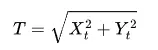
where T is the true error radius caused by translational error; is the error along the X - axis; is the error along the Y - axis.
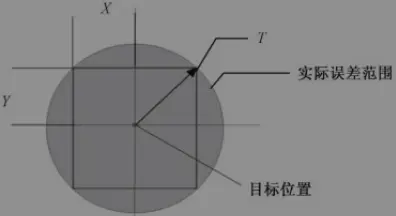
(2) Rotational Error
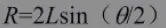
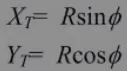
The rotational error is caused by the error of the component positioning mechanism and the rotational error of the Z - axis. The definition of rotational error is the angular deviation between the theoretical position and the actual position, such as the angle θ in the following figure. Since the vertex corresponding to the diagonal of a rectangular component is the farthest from the center of the component, the rotational error at this point is the largest. For the convenience of analysis, as shown in the above figure, when the rotational error is θ, the distance R that the vertex of the diagonal of the component moves is called angular displacement, which can be given by the following formula:
(where the angle θ is in radians)
where R is the angular displacement; L is the length of the diagonal of the rectangular component; θ is the rotational error. Sometimes, the rotational error needs to be expressed by the errors in the X - axis and Y - axis directions, which can be obtained from the following equations for the X - Y error components:
where is the X - axis error caused by rotational error; is the Y - axis error caused by rotational error; R is the angular displacement; φ is the angle between the X - axis and the angular bisector of the rotational error θ.
(3) Total Error
When actually mounting components, rotational error and translational error exist simultaneously. In this case, a combined cumulative effect is generated. The total error is obtained by the vector addition of these two components. The total error components of the X - axis and Y - axis can be obtained from the following formula:
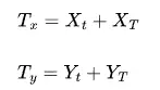
Then the total error is obtained by the following formula:
where , are the total error components of the X - axis and Y - axis; , , and are as defined above.
Since the influence of rotational error depends on the size of the component, it is necessary to determine the translational error and rotational error separately. After selecting the type of component to be mounted, the total mounting accuracy can be calculated from these two values.
2、IPC Standard Regulations on Mounting Accuracy
(1) Classification of Electronic Products
In the IPC standard, electronic products are divided into the following three levels.
Level 1: General consumer electronics products. These products are used in a relatively stable environment, requiring a high peRFormance - to - price ratio and low cost, and the requirement for reliability is not very high.
Level 2: Industrial and commercial electronics products. The use environment of these products varies greatly. They require both a high performance - to - price ratio and a long service life, and the reliability requirement is relatively high.
Level 3: High - reliability electronic equipment. The continuous performance of these products is crucial, and malfunctions such as downtime are not tolerated. The user's environment may be harsh. This type of product includes high - reliability products such as life - saving equipment and military equipment, and the impact of each product is different.
(2) Relevant Standards of IPC - A - 610
During SMT mounting, the ideal state is that the leads of the component completely coincide with the pads on the circuit board. However, during the mounting process, due to factors such as the positioning deviation of the circuit board, the deviation of component picking, the deviation of correction, the deviation of the machine positioning system, and environmental factors, this ideal state is difficult to achieve.
IPC - A - 610 is the acceptable standard for the offset error between components and pads after the printed circuit board assembly and soldering of three - level electronic products. Taking chip components and SOP components as examples, it is simply summarized as follows.
For Level 1 and Level 2: The overlapping part (C) of the width of the component's solder end or lead width (W) and the width of the pad on the circuit board (P) should account for at least 50% of the width of the component or the pad (as shown in the following figure).
For Level 3: The overlapping part (C) of the width of the component's solder end or lead width (W) and the width of the pad on the circuit board (P) should account for at least 75% of the width of the component or the pad (as shown in the following figure).
(3) Relevant Provisions of IPC9850 Standard
IPC - A - 610 only makes acceptability provisions for the offset of component leads and the PCB after welding, without involving the offset error after mounting and the welding process method. In fact, if the reflow soldering process is used, since the components are in a "suspended" state during the welding process, due to the wetting force, reflow soldering has a "self - calibration" effect, that is, the components have the effect of reducing the offset error after welding. According to the principle of taking the data in the most unfavorable state in error measurement and calculation, for the evaluation of mounting accuracy, we can only consider the offset error during mounting.
In the requirements for the accuracy of the chip mounter in the IPC9850 standard, in addition to the accuracy requirements for the X, Y, and θ axes of the machine, a comprehensive consideration method is also proposed, that is, the influence of the combination of all axis deviations on the accuracy of the chip mounter. The basic basis of this method is that many errors are caused by the combined error of appropriately sized X, Y, and θ mounting errors, and are by no means caused by only one of them. This method considers the comprehensive influence of the three errors and is called Overhang or Superposition (coincidence degree). In fact, it has been found that when the X, Y, and θ axis deviations are considered separately, they can meet the specified requirements, but when combined, sometimes a qualified welding connection cannot be formed.
The advantages of this method are obvious. It is closer to the actual assembly process than the traditional view that the performance of each axis is considered independently, because the mounting accuracy is ultimately reflected in the product quality evaluation after welding.
In the comprehensive consideration of the X, Y, and θ axis errors in IPC9850, two quantities, total error and lead - pad coincidence degree, are used. The total error is the maximum amount of the outer end error of the lead, which is related to the lead - pad coincidence degree. The specific calculation can refer to the IPC9850 standard "3.3.3.2.2 Cpk for Termination - to - Land Coverage". In the actual measurement of the accuracy of the chip mounter, the total error corresponds to the lead - pad overhang amount. For example, for a QFP with a lead width of 0.2mm, requiring the total error (for leaded components, it is MLTE) ≤ 0.100 is equivalent to requiring the lead - pad coverage rate ≥ 75%. A total error limit of 0.15 corresponds to LTL ≥ 50%. For detailed regulations and calculations, please refer to the relevant IPC standards.
3、Requirements for the Accuracy of the Chip Mounter for Mounting Miniature Components
The requirements for the accuracy of the chip mounter for mounting miniature components vary according to the product type. When the product is required to meet the Level 3 standard, assuming that the width of the component pad or lead is the same as that of the pad on the circuit board, for mounting a 01005 (0.4mm×0.2mm) component, the machine accuracy must reach 0.05mm; for mounting a component with a 0.4mm lead pitch and a lead width of 0.2mm, the machine accuracy must also reach 0.05mm.
(1)Analysis of SMT Mounter Mounting Precision Parameters and How to Measure Them
(2)Analysis of SMT Mounter Mounting Precision Parameters and How to Measure Them