 PCB
PCB FPC
FPC Rigid-Flex
 FR-4
FR-4 HDI PCB
 Rogers High-Frequency Board
 PTFE Teflon High-Frequency Board
 Aluminum
 Copper Core
 PCB Assembly
 LED light PCBA
 Memory PCBA
 Power Supply PCBA
 New Energey PCBA
 Communication PCBA
 Industrial Control PCBA
 Medical Equipment PCBA
 Testing Service
 PCBA Testing Service
 Certification Application
 RoHS Certification Application
 REACH Certification Application
 CE Certification Application
 FCC Certification Application
 CQC Certification Application
 UL Certification Application
 Transformers, Inductors
 High Frequency Transformers
 Low Frequency Transformers
 High Power Transformers
 Conversion Transformers
 Sealed Transformers
 Ring Transformers
 Inductors
 Wires,Cables Customized
 Network Cables
 Power Cords
 Antenna Cables
 Coaxial Cables
 Net Position Indicator
 Solar AIS net position indicator
 Capacitors
 Connectors
 Diodes
 Embedded Processors & Controllers
 Digital Signal Processors (DSP/DSC)
 Microcontrollers (MCU/MPU/SOC)
 Programmable Logic Device(CPLD/FPGA)
 Communication Modules/IoT
 Resistors
 Through Hole Resistors
 Resistor Networks, Arrays
 Potentiometers,Variable Resistors
 Aluminum Case,Porcelain Tube Resistance
 Current Sense Resistors,Shunt Resistors
 Switches
 Transistors
 Power Modules
 Isolated Power Modules
 AC-DC Power Modules
 DC-AC Module(Inverter)
 RF and Wireless
Allowable Warpage Tolerance of PCBs after Reflow Soldering: A Comprehensive Analysis
Abstract: Post-reflow PCB warpage critICally impacts assembly yield, solder joint reliability, and product longevity. According to international standards (e.g., IPC) and application scenarios, the allowable warpage typically ranges from 0.3% to 1.5%, depending on component density, board thickness, and process requirements.
1. Standard Definitions and Key Parameters
-
Warpage Calculation Formula:
Warpage (%) = (Maximum Deformation Height / Diagonal Length) × 100%
Measurement: Follows GB4677.5-84 or IPC-TM-650.2.4.22B by placing PCB on a calibrated platform and inserting a probe at the maximum deformation point. -
General Standards:
-
SMT Boards: ≤0.75% (IPC-6012).
-
Non-SMT Boards: ≤1.5%.
-
High-Density Boards (BGA/Fine-Pitch ICs): ≤0.5%, with some manufacturers requiring ≤0.3%.
-
-
Thickness Impact:
-
Risk decreases significantly when thickness ≥1.6mm;
-
Thin boards (≤0.8mm) require special processes (e.g., clamped rollers during plating) to avoid 40% higher deformation.
-
2. Application-Specific Requirements
| Scenario | Allowable Warpage | Critical Constraints | Standard |
|---|---|---|---|
| Standard SMT | ≤0.75% | Prevents cold joints/misalignment | IPC-6012 |
| BGA/0.2mm Pitch | ≤0.5% | Bridging risk ↑40% | In-house standards |
| Aerospace/Military | ≤0.5% | Anti-deformation mounting causes via fractures | GJB3835 |
| Flexible Pcbs (FPC) | ≤0.75% | Requires lamination compensation; SMO-to-copper ≥0.15mm | IPC FPC supplements |
Note: Warpage >0.75% prohibits forced anti-deformation mounting; use local shimming to relieve stress.
3. Failure Mechanisms and Consequences
-
Soldering Defects:
-
Warpage >0.5% increases BGA voiding by 30% and tombstoning/cold joint risk by 5×.
-
Board bending causes uneven solder paste deposition, dielectric loss deviation >8%.
-
-
Structural Damage:
-
Forced installation in chassis rails shears plated through-holes in multilayer PCBs.
-
Solder mask bridge fractures induce moisture corrosion and insulation failure.
-
-
Assembly Failures:
-
Warpage >0.3% risks damaging pick-and-place machines and increases misinsertion by 50%.
-
4. Process Control Methods
-
Material Optimization:
-
High-Tg Substrates: Tg≥170°C (vs. 130°C for standard FR-4), reducing Z-axis CTE by 50% and enhancing thermal resistance.
-
Balanced Copper Design: A/B-side copper area difference <10%, otherwise add grids for compensation.
-
-
Design Improvements:
-
Replace V-Cut with Router scoring to preserve structural integrity.
-
Symmetric prepreg stacking in multilayer boards (e.g., identical 1-2/5-6 layer thickness for 6-layer PCBs).
-
-
Process Adjustments:
-
Stress Relief Baking: 150°C for 4 hours post-lamination; 8±2 hours pre-cutting.
-
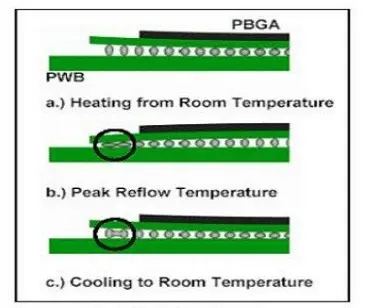
Reflow Profile: Ramp rate ≤2°C/sec (prevents ceramic capacitor micro-cracks), cooling rate ≤4°C/sec.
-
Reflow Carriers: Double-sided carriers reduce deformation by 80% but increase cost by 30%.
-
5. Inspection and Correction Techniques
-
In-Line Monitoring:
-
3D Laser Microscopy: 0.1μm precision for real-time warpage feedback.
-
Dual-Threshold AOI: Strict standard ±0.005mm (high-density areas), acceptable standard ±0.008mm.
-
-
Correction Methods:
-
Over-tolerance boards (>0.75%) baked at 150°C under pressure for 3–6 hours salvage 60% of mildly warped PCBs.
-
Natural cooling on marble slabs after hot-air leveling avoids thermal shock from water quenching.
-
Conclusion
Post-reflow PCB warpage control requires design-material-process synergy:
-
General Use: ≤0.75% (IPC baseline); high-density boards must achieve ≤0.5%.
-
Core Principle: Suppress stress via copper balancing, high-Tg materials, and baking; combine LDI (±0.015mm accuracy) with dynamic compensation for micron-level control.