 PCB
PCB FPC
FPC Rigid-Flex
 FR-4
FR-4 HDI PCB
 Rogers High-Frequency Board
 PTFE Teflon High-Frequency Board
 Aluminum
 Copper Core
 PCB Assembly
 LED light PCBA
 Memory PCBA
 Power Supply PCBA
 New Energey PCBA
 Communication PCBA
 Industrial Control PCBA
 Medical Equipment PCBA
 Testing Service
 PCBA Testing Service
 Certification Application
 RoHS Certification Application
 REACH Certification Application
 CE Certification Application
 FCC Certification Application
 CQC Certification Application
 UL Certification Application
 Transformers, Inductors
 High Frequency Transformers
 Low Frequency Transformers
 High Power Transformers
 Conversion Transformers
 Sealed Transformers
 Ring Transformers
 Inductors
 Wires,Cables Customized
 Network Cables
 Power Cords
 Antenna Cables
 Coaxial Cables
 Net Position Indicator
 Solar AIS net position indicator
 Capacitors
 Connectors
 Diodes
 Embedded Processors & Controllers
 Digital Signal Processors (DSP/DSC)
 Microcontrollers (MCU/MPU/SOC)
 Programmable Logic Device(CPLD/FPGA)
 Communication Modules/IoT
 Resistors
 Through Hole Resistors
 Resistor Networks, Arrays
 Potentiometers,Variable Resistors
 Aluminum Case,Porcelain Tube Resistance
 Current Sense Resistors,Shunt Resistors
 Switches
 Transistors
 Power Modules
 Isolated Power Modules
 AC-DC Power Modules
 DC-AC Module(Inverter)
 RF and Wireless
Achieving Vertical Interconnects in 2.5D/3D Packages via Through-Silicon Via (TSV) Technology
1. TSV Fundamentals and 2.5D/3D Architectures
Through-SilICon Via (TSV) enables vertical interconnects through silicon substrates, critical for chip stacking (3D) or interposer-based integration (2.5D). Key advantages include:
-
Shorter interconnects: TSVs reduce delay by >50% compared to wire bonding;
-
High bandwidth: TSV density up to 10⁴–10⁵/cm² supports HBM2e (1024-bit I/O);
-
Heterogeneous integration: Combines logic, memory, and photonic devices.
2.5D: Silicon interposers (50–100 μm thick) connect multiple chips to organic substrates (e.g., FCBGA).
3D: Direct chip stacking (e.g., DRAM-on-Logic) with TSVs for layer-to-layer connections.
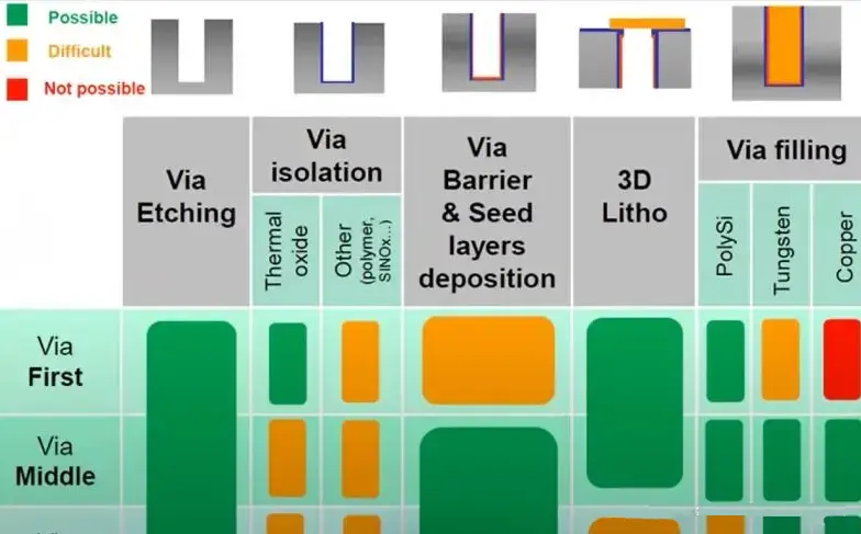
2. TSV Fabrication Process and Key Technologies
(1) Deep Reactive Ion Etching (DRIE)
-
Bosch process: Alternating SF₆ etch and C₄F₅ passivation achieves high aspect ratios (AR=10:1–20:1) with Ra <50 nm;
-
Laser drilling: For ultra-thin wafers (<50 μm) or glass vias (TGV), requiring post-CMP polishing.
(2) Insulation and Barrier Deposition
-
Insulation: PECVD SiO₂ (0.5–1 μm) or ALD Al₂O₃ (10–20 nm) for voltage isolation;
-
Barrier: PVD Ta/TaN (50 nm) to block Cu diffusion.
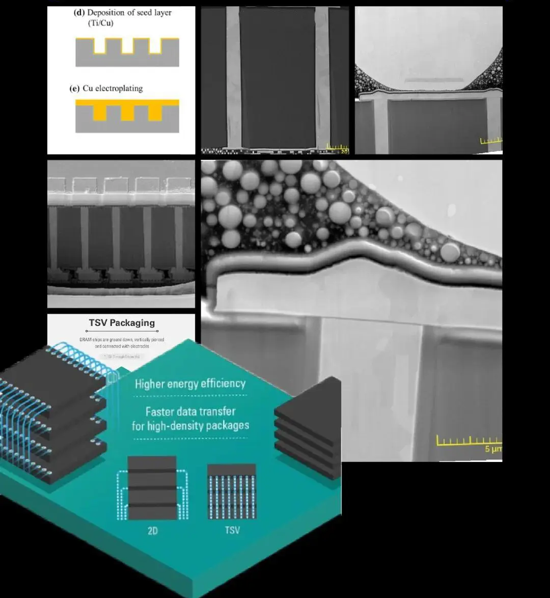
(3) Seed Layer and Electroplating
-
Seed layer: IMP-enhanced PVD Cu (200–500 nm) for sidewall coverage;
-
Electroplating:
-
Void-free filling via PRC with SPS/PEG additives;
-
Annealing (200–250°C) reduces resistivity to 2–3 μΩ·cm.
-
(4) Thinning and Bonding
-
Temporary bonding/thinning:
-
Grind wafers to 20–50 μm thickness using WaferBOND®;
-
XeF₂ dry etch or CMP to expose TSV Cu pillars.
-
-
Hybrid bonding:
-
Cu-Cu bonding (300–400°C, 10–50 MPa) for <10⁻⁸ Ω·cm² resistance;
-
Oxide bonding for mechanical support.
-
3. Critical Challenges and Solutions
(1) Thermal Stress Management
-
Challenge: CTE mismatch (Si: 2.6 ppm/°C vs. Cu: 17 ppm/°C) causes fatigue;
-
Solutions:
-
Annular TSVs with low-CTE polymers (e.g., BCB);
-
FEA-optimized layouts (stress <100 MPa).
-
(2) Signal/Power Integrity
-
SI: Shielded differential TSV pairs reduce crosstalk (>20 dB @10 GHz); TLM models for 50±5 Ω impedance.
-
PI: Embedded MLCCs (impedance <1 mΩ @100 MHz) and 3D power grids.
(3) Testing and Reliability
-
Electrical tests: 4PP for resistance (<50 mΩ/TSV); TDR for SI validation.
-
Reliability tests:
-
Thermal cycling (-55–125°C, 1000×) with <5% resistance drift;
-
HAST for Cu diffusion evaluation.
-
4. Advanced Trends and Applications
(1) Microbumps and Hybrid Bonding
-
Cu-Sn microbumps (5–10 μm diameter) for HBM-GPU integration;
-
Hybrid bonding (Cu/SiO₂) enables 10⁶/cm² density in 3D NAND.
(2) Photonic Integration
-
Silicon photonic interposers with TSVs and waveguides for CPO Modules (<1 dB/cm loss).
(3) Cost Control
-
Multi-project wafers (MPW) for mask sharing;
-
Wafer-level packaging (WLP) reduces per-chip steps.