 PCB
PCB FPC
FPC Rigid-Flex
 FR-4
FR-4 HDI PCB
 Rogers High-Frequency Board
 PTFE Teflon High-Frequency Board
 Aluminum
 Copper Core
 PCB Assembly
 LED light PCBA
 Memory PCBA
 Power Supply PCBA
 New Energey PCBA
 Communication PCBA
 Industrial Control PCBA
 Medical Equipment PCBA
 Testing Service
 PCBA Testing Service
 Certification Application
 RoHS Certification Application
 REACH Certification Application
 CE Certification Application
 FCC Certification Application
 CQC Certification Application
 UL Certification Application
 Transformers, Inductors
 High Frequency Transformers
 Low Frequency Transformers
 High Power Transformers
 Conversion Transformers
 Sealed Transformers
 Ring Transformers
 Inductors
 Wires,Cables Customized
 Network Cables
 Power Cords
 Antenna Cables
 Coaxial Cables
 Net Position Indicator
 Solar AIS net position indicator
 Capacitors
 Connectors
 Diodes
 Embedded Processors & Controllers
 Digital Signal Processors (DSP/DSC)
 Microcontrollers (MCU/MPU/SOC)
 Programmable Logic Device(CPLD/FPGA)
 Communication Modules/IoT
 Resistors
 Through Hole Resistors
 Resistor Networks, Arrays
 Potentiometers,Variable Resistors
 Aluminum Case,Porcelain Tube Resistance
 Current Sense Resistors,Shunt Resistors
 Switches
 Transistors
 Power Modules
 Isolated Power Modules
 AC-DC Power Modules
 DC-AC Module(Inverter)
 RF and Wireless
EMC's problems and countermeasures in PCB design
EMC's problems and countermeasures in Pcb Design
In the design process of electronic products, electromagnetic compatibility (EMC) is a crucial consideration. EMC issues not only affect product peRFormance, but also may cause serious electromagnetic interference, resulting in equipment failure or data loss. Especially in the design ofprinted circuit boards (PCB), EMC issues are particularly prominent, mainly including conducted interference, crosstalk interference, and radiated interference.
I. Basic concepts and main interference types of EMC
EMC refers to the ability of a device or system to operate normally in its electromagnetic environment without causing unacceptable electromagnetic interference to anything in that environment. In PCB design, common EMC issues mainly include the following three types:
Conducted interference
Conducted interference is a form of interference that affects other circuits through lead wires or common-mode impedance decoupling. For example, when noise enters the system through the power supply circuit, the support circuit will be affected by the noise. This interference usually occurs between power lines and ground lines, propagating through common impedance.
Crosstalk interference
Crosstalk interference refers to the interference of one signal line to adjacent signal lines. It usually occurs on adjacent circuits and conductors. Due to the mutual capacitance and mutual impedance between circuits and conductors, when a signal propagates on one wire, it will induce current on adjacent wires, causing interference.
Radiation interference
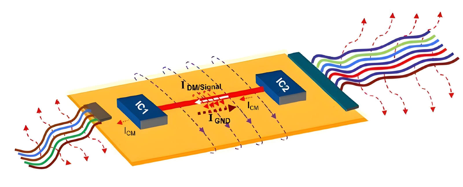
Radiated interference is interference caused by radiation emitted by free electromagnetic waves. In PCBs, this interference is usually manifested as common-mode radiation interference between cables and internal lines. When electromagnetic waves are irradiated on the transmission line, a decoupling problem of the electric field on the line will occur, resulting in the division of small voltage sources on the line into common mode CM and differential mode DM currents.
II. Strategies for reducing EMC problems
In order to effectively reduce the occurrence of EMC problems, the following strategies can be adopted in PCB design:
Use a low inductance grounding system
A low-inductance grounding system is an effective means of reducing electromagnetic radiation and interference. By maximizing the ground contact area on the PCB, the ground inductance in the system can be reduced. In PCB design, it is best to use one of the layers as a ground plane to provide a low-impedance path. If it is not possible to ground the entire floor, a grounding grid can be used, but the grounding inductance will depend on the space between the grids.
Components are placed according to their functions
In order to reduce interference between different functional circuits, components on the PCB should be grouped according to function, such as analog circuits, digital circuits, power supply circuits, low-speed circuits, and high-speed circuits. The signal traces of each component must be kept within a defined area to reduce cross-area interference. When signals need to be connected from one subsystem to another, filters can be used for isolation.
Reasonably arrange the number of PCB layers
The EMC performance of PCB also depends on the arrangement of its layers. For a 2-layer PCB, the entire layer should be used as a ground plane as much as possible. For PCBs with 4 or more layers, alternating ground and signal layers should be used to avoid EMC issues. For example, in a 4-layer PCB, the layers below the ground plane should be used as power planes, while the top and bottom layers are used as signal planes.
Add decoupling capacitor
Decoupling capacitors can reduce the propagation of switching noise on the PCB and direct the noise to ground. When ICs are working, due to their internal structure, they switch at high frequencies, generating switching noise in the IC connection tracks. By placing a decoupling capacitor near the IC, the impact of this noise on the system can be effectively reduced.
Avoid crosstalk
In order to reduce crosstalk interference, various measures can be taken. For example, using differential signal transmission, increasing the distance between traces, and reducing the speed of traces. In addition, shielding layers or ground planes can be used to isolate adjacent traces to reduce electromagnetic coupling between them.

Avoid 90° routing
A 90° track turn at a right angle will increase parasitic capacitance, leading to changes in characteristic impedance and thus causing reflections. Therefore, in PCB design, one should avoid using right-angle bends and instead use 45° bends to limit noise coupling to nearby traces. At the same time, the width of the signal trace should be kept constant from the source to the load to avoid reflections caused by impedance changes.

Line separation
Wiring separation is an effective means to reduce crosstalk and electromagnetic coupling. The general rule is that the spacing between traces, measured from center to center, should be greater than or equal to 3 times the trace width. The larger the spacing, the lower the crosstalk and coupling. For specific cases where more parallel traces are required and the spacing is minimal, coplanar waveguides (CPW) can be used to reduce crosstalk between signal traces on different layers.
The via hole is far away from the key signal routing
Vias are used for signal routing in multilayer PCBs, but if not designed properly, they can introduce parasitic capacitance and inductance effects. Therefore, avoid placing vias too close to critical traces. When it is unavoidable, ensure that the grounding via is placed close to the signal via to reduce changes in characteristic impedance and reflection.
Place a reference plane near the trace
Placing a reference plane near the trace can prevent radiated EMI. This applies to both all-digital and mixed-signal systems. When routing, ensure that the signal traces have a clear return path and use reference plane layers to provide isolation. For impedance control systems, coplanar grounding arrangements can also be used to further reduce interference.
By implementing the above strategies, the EMC problems in PCB design can be significantly reduced, and the electromagnetic compatibility and reliability of the product can be improved. However, due to the complexity and diversity of EMC issues, designers also need to respond flexibly and continuously improve based on actual conditions.